The R-S latch is a simple form of sequential circuit, but
one which has few practical uses. A much more useful type is the edge-triggered
D-type flip-flop, which is represented in a diagram by the symbol of Figure
4.1. The internal circuit consists of gates coupled to each other,
but all we need to know about the circuit is the overall action of the i.c.,
since the D-tpe flip-flop is too complex to be worth building up from
separate (discrete) components.
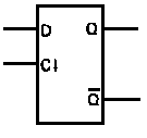 |
Figure 4.1. Symbol for a D-type
flip-flop |
The i.c. has two main inputs, D and Clock, and outputs Q and
Q These outputs are always inverse to each other, they can never be
identical unless the circuit has failed. The D (for Data) input consists
of a logic signal, 1 or 0, and the clock input is the usual clock pulse described
in Chapter 3. The usual action of the D-type flip-flop is that the logic
signal voltage at the D input is switched to the Q output by the
leading edge of the clock pulse. For example, if the D input were
at logic 1 before the clock pulse arrived, and the Q output were at logic
0, then the output would be switched over to logic 1 at the leading edge
of the clock pulse. Most designs of D-type flip-flops 'lock-out' data during
the high part of the clock pulse. This means that the switchover is completed
by the time the clock pulse has reached logic 1, and any change of voltage
at the D input has no effect on the Q output during the rest of the cycle,
the high part of the clock pulse, the trailing edge and the time between
pulses.
The D-type flip-flop is very useful as a latch because rapidly-hanging data
signals can be 'captured' at the leading edge of each clock pulse to the
D-type. A digital figure readout, for example, must not change rapidly while
it is being viewed, so a latch of some sort may be needed to keep the displayed
figures steady while a reading is taken. The latching action enables a bit
of data to be stored for a time equal to the time between clock pulses, no
matter how the input signal varies in this time.
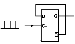 |
Figure 4.2. Toggling connection to make
the D-type into a binary counter |
A very important circuit action can be achieved by connecting
the Q output back to the D input as shown in Figure 4.2 and using
the clock input only. Remember that the Q output signal will always
be the inverse of the Q output signal, and imagine that the Q output is at
logic 0,so that the Q output is at logic 1. This sets the D input
at logic 1 so that the leading edge of the next clock pulse will switch the
flip-flop over, making the Q output change to logic 1. This does not happen
instantly, however, there is a delay of around 40 ns, a very short time but
long enough to ensure that the clock signal has fully reached logic 1 before
the outputs change voltage. By the time the Q output has changed to 1 and
the Q to 0, the clock pulse has reached logic 1, and data is locked
out. The logic 0 signal at Q therefore has no effect on the
D input until the leading edge of the next clock pulse. At this next clock
pulse, the 0 at the D input will cause the Q output to switch to 0, and the
Q to 1, but again with enough delay to ensure that the change at Q
has no effect on the D input.
Clock |
Qn-1 |
Qn |
Dn |
_
Qn |
| 1 |
0 |
1 |
0 |
0 |
| 2 |
1 |
0 |
1 |
1 |
| 3 |
0 |
1 |
0 |
0 |
|
Figure 4.3. Truth table for a toggled D-type.
The Q output changes over at each clock pulse |
Clock input and Q output signals for a D-type connected in this way are shown
in Figure 4.3. Two complete pulses at the clock input produce one
complete pulse at the Q output, so that this circuit is variously known as
a scale-of-two, divide-by-two or binary counter.
The D-type flip-flop becomes more useful if two additional inputs are available.
One of these is labelled. 'set' or 'preset' and is used to force the Q output
to logic 1 no matter what the state of the clock pulse happens to be. The
other input is labelled 'reset' or 'clear', and its action is to force the
Q output to logic 0. These inputs are sometimes called asynchronous
inputs, because a signal to either of these inputs need not be synchronised
in any way with the clock signal. Precautions have to be taken (by gating,
for example) to ensure that both inputs are not operated at the same time.
Most TTL flip-flops need a negative-going pulse to operate the preset/set
and reset/clear inputs.
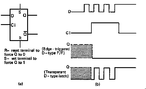 |
Figure 4.4. D.type variations: (a) using
reset (clear) and set (preset) terminals to fix the Q outputs irrespective
of the clock, (b) the D-type edge-triggered flip-flop compared to the transparent
latch. The output of the latch will correspond to the state of the D input
for as long as the clock Is at logie 1. The shading indicates where the Q
output may be 1 or 0 depending on how the output was previously
set |
The name D-type is also used for a type of latch in which binary
digits at the D input are gated to the output only while the clock pulse
is at logic 1, and are stored (latched) while the clock pulse is at logic
0. This D-type latch cannot be used in the same way as the edge-triggered
flip-flop. It would be feasible to construct a D-type flip-flop which was
triggered by the trailing edge of the clock pulse, but the leading-edge type
is the one generally used.
The J-K flip-flop
The D-type flip-flop, though useful, has several disadvantages which have
led to a more versatile circuit, the J-K master-slave flip-flop. The connections
to a typical J-K are shown in Figure 4.5. Besides the usual clock
input, there are two inputs labelled 'J' and 'K' respectively which control
the action of the flip-flop when the clock pulse arrives. Two other inputs,
as noted above, labelled 'set' (or 'preset') and 'reset' (or 'clear') control
the output of the flip-flop whether a clock pulse has arrived or not. The
usual outputs are Q and Q.
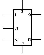 |
Figure 4.5. J-K flip-flop input and outputs
The S (set) input is sometimes labelled P (preset) and the R (reset) input
is sometimes labelled C (clear) |
The internal action of a J-K master-slave flip-flop is rather
complicated but basically the circuit consists of two flip-flops. The first
flip-flop (master) is operated by the leading edge of the clock pulse, and
its output is controlled by the settings of the J and K inputs at this instant.
The outputs of this master flip-flop are connected to the inputs of the second
flip-flop (slave), which switches over on the trailing edge of the clock
pulse. The outputs of the slave flip-flop are Q and Q, so that these
outputs change only at the trailing edge of the clock.
This provides a 'lockout' system which neither depends on the delays in the
circuit nor needs such a fast-rising pulse as the D-type. Data at the J
and K inputs is transferred to the master at the clock leading edge, and
after this time changes at these inputs have no effect. The outputs change
at the trailing edge of the clock, so that any connection back from output
to input has no effect until the next clock pulse arrives. Figure 4.6
shows a timing diagram.
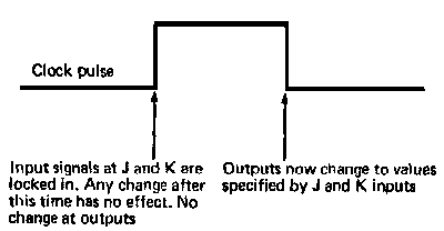 |
Figure 4.6. The timing of events in
a J-K master-slave flip-flop |
The most significant advantage of the J-K flip-flop is its
versatility because of the control exerted by the J and K inputs. Figure
4.7 shows a truth table, with Q referring to the Q output voltage before
the clock pulse arrives, and Qn+1 the output voltage after
the clock pulse. Though the truth table summarises what happens, the
action is so important that we shall go over it in detail. With J = 0, K
= 0, the logic signal at the Q input is unchanged at the clock pulse, so
that the flip-flop can be set to latch for as long as J = 0, K= 0.
| J |
K |
Q |
Qn+1 |
| 0 |
0 |
0 |
0 |
| 1 |
1 |
| 0 |
1 |
0 |
0 |
| 1 |
0 |
| 1 |
0 |
0 |
1 |
| 1 |
1 |
| 1 |
1 |
0 |
1 |
| 1 |
0 |
|
| Figure 4.7. Truth table for a J-K master-slave
flip-flop |
With the inputs set at J=1, K 0, the output Q will switch to
logic 1 when clocked (or remain at 1 if that was its previous value). Input
settings of J=0, K = 1 will cause the Q output to switch to logic 0 when
clocked or to remain at 0 if that was its previous value.
When the J and K inputs are set to J= l,K= l,the Q output voltage will reverse
at each clock pulse, producing the same counting action as the back-connected
D-type flip-flop of Figure 4.2, so that the J-K flip-flop can be used
as a binary counter without the need to make any feedback connections.
As noted earlier, the asynchronous inputs labelled 'set/preset' and 'reset/clear'
can be used to switch the Q output to either logic voltage irrespective of
the clock voltage.
Three-state latches
A variation of the latch is the three-state latch, a circuit which
is particularly important in microprocessor circuits. A three-state latch
performs the usual latching function of retaining a signal at its output
after the inputs have changed, but with the addition of an enable
pin. When the enable pin voltage is switched, the outputs of the latch are
isolated, floating, and free to take up either logic voltage. This 'third
state' is needed' when signals can pass along lines in either direction,
and avoids the difficulties which could arise if one device were at logic
1 and another connected to the same line were at logic 0. The enabling signal
must be generated so that the latch is 'floated' whenever the lines are being
used for other signals. Quad (four line.4), hex (six lines) and octal (eight
lines) latches are available in three-state form, and 'enable high' or 'enable
low' types can be selected. Examples include the 74125 and 74126 (quad);
74365 and 74367 (hex).
Binary counters
A binary counter is a circuit whose input is a series of pulses and whose
output is binary digits, with a separate line for each power of two,
20, 21, 22, 23 and so on. The
simplest type of binary counter is a chain of connected flip-flops such as
that Figure 4.8.
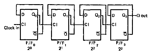 |
Figure 4.8. A binary counter chain of
flip-flops.This type is of circuit is known as a ripple, (or asynchronous
) counter |
A binary counter chain of flip-flops. This type of circuit is
known as a ripple (or asynchronous) counter shown in Figure 4.8 (in
which D-type flip-flops are shown). A counter of this type is variously known
as a ripple, ripple-through or asynchronous counter.
Imagine that we have a chain of flip-flops which change state on the trailing
edge of the clock. At each flip-flop Q output an led. is connected so that
the led. will glow when Q = 1. Imagine that all the l.e.d.s are extinguished
at the start of counting. When the first pulse arrives, flip-flop 0 is switched
over, so its Q0 output is high (Figure 4.9) and its l.e.d.
glows. Since this type of flip-flop switches over on the trailing edge of
the clock pulse, flip-flop l is not switched over by the rise of Q0
from 0 to 1. A second pulse into flip-flop 0, however, will cause this
flip-flop to switch again, so that its output voltage drops from 1 to 0.
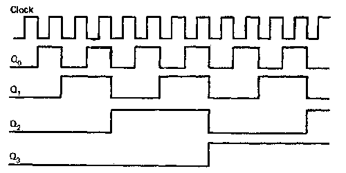 |
Figure 4.9. Timing diagram for a binary
counter, assuming that all the flip-flops were reset (cleared) before
starting |
This is a trailing edge, so flip-flop 1 is switched and its
Q1 output rises to logic 1, lighting the second l.e.d. At the
same time, the first l.e.d. is extinguished by the drop in voltage of
Q0. A third pulse in will now cause the first l.e.d. to light
again, leaving the second l.e.d. unaffected. A fourth pulse will extinguish
l.e.d.s 1 and 2 but switch on l.e .d. 3.
The reason for numbering the flip-flops 0, 1,2 rather than 1, 2, 3 now becomes
apparent. Flip-flop 0 counts the binary columns 20, flip-flop
1counts 21 etc., so that the l.e.d.s can be read as a set of binary
1s, each showing a different power of 2 as indicated in Figure 4.10.
If a gate is now added to the system (Figure 4.10) the counter is
nearly complete. With all flip-flops set to give 0 output (no l.e.d.s lit)
the gate is opened (enabled). Later the gate is closed and the number of
pulses that have passed through the gate will be recorded by the l.e.d.s
of the counter.
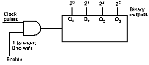 |
Figure 4.10. Adding a gate to the binary
counter so that counting can be stopped and started by an 'enable'
voltage |
We can also regard this as a memory circuit which can be set
to a binary digit (read from the most significant digit downwards) which
will remain until either it is reset or more pulses are added. Another way
of looking at the circuit is as a serial adder, adding the number of pulses
at the input to any number that has been set by a previous input.
The circuit may be used purely as a binary counter, with any number of flip-flops
- a common number is four or eight. Alternatively, the circuit may be modified
to count in other ways. Imagine, for example, that a BCD counter is needed.
Such a counter must produce a binary count for up to nine pulses, but must
reset to 0 at the tenth pulse, passing on this tenth pulse to the next BCD
stage as a 'carry'.
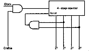 |
Figure 4.11. Converting a four-stage
counter Into a BCD counter by resetting at the instant when decimal 10 (binary
1010)is detected at the outputs |
For a count up to nine, four flip-flops will be needed, and
if J-K-type master-slave flip-flops, such as the 7476, are used the resetting
can be carried out by using the reset (clear) inputs. How can we use the
tenth pulse to operate the reset? The simplest solution is to use a gate
circuit which will detect decimal 10 and give an output which operates the
reset. The reset action of the flip-flop requires a negative-going pulse
on the reset pin,
so that a gate which will have a 1-to-0 change when decimal is counted
can carry out the resetting action that we need.
Such a circuit is shown in Figure 4.11. Since decimal 10 is binary
1010, a NAND gate operated by the 23 and 21 outputs
of the counter will produce a 1-to-0 change which can be used to operate
the reset. Whenever the reset operates, the voltage on the reset pin must
then be restored so that counting can restart, so the reset pin is pulsed
only very briefly negative. An inverter can convert this brief negative pulse
into a positive pulse which can be counted by the next set of BCD flip-flops.
Using gates to control the reset inputs of a chain of flip-flops is a simple
and straightforward way of adjusting the maximum count figure, but it is
not an ideal method. When high counting speeds, or a large number of stages,
are to be used then the time delay for a pulse to 'ripple through' becomes
excessive. For example, consider a counter with eight flip-flops, when the
count has reached 01111111. The next pulse in will change the least significant
digit from l to 0, and this in turn will change the next digit from 1 to
0 and so on, until the last digit is changed from 0 to 1. Now there
is a measurable delay, 25 ns or more, between the action of the clock pulse
and the change at the output, so these changes are not immediate but foflow
on each other, hence the expression 'ripple-through'.
It would be quite possible to have a circuit arranged to detect the state
10000001 by connecting the 27 and 20 outputs to a NAND
gate input which in turn activated reset. If the clocking rate were fast,
however, the early stages of the circuit could have counted several more
pulses before the final flip-flop switched over, so that the actual count
would not be consistent. The circuit would behave well at low pulse rates,
but would give erratic counting at high speeds due to the delays. For this
reason ripple counters are not used for applications of this type, though
they have one outstanding advantage for high-speed counting. Their advantage
is that only the first flip-flop servicing the least significant digit has
to run at the high speed of the input pulses. The next flip-flop
(21) runs at half input speed, and so on. If the counter is used
purely as a precise frequency divider, or to register the number of counts
on a binary readout after pulses have been shut-off, then the ripple counter
is ideally suited.
A ripple counter need not necessarily count up,that is from 0 up to whatever
maximum value is set by the design. A down-counting ripple counter can be
constructed simply by connecting the Q outputs of each flip-flop to the clock
input of the next in line, as shown in Figure 4.12.
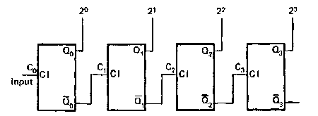 |
Figure 4.12. A down-counter constructed
by connecting each Q output to the next clock input. Only the
Q-to-clock connections are shown here |
Imagine that the Q outputs have started at the number 1111
(binary), which is 15 (decimal). The first complete pulse into C0
will switch Q0 from 1 to 0 and Q0 from 0 to 1.
The reading of the outputs is now 1110 (remember that C0 carried
the least significant bit) which is 14 (decimal). The next complete pulse
will switch Q0 high again, but with Q0 changing from
1 to 0, C1 will be triggered so that its output falls from 1 to 0. The read-out
is now 1101, decimal 13. This countdown will, continue until the outputs
reach 0, when the next pulse resets the counter to 1111.
A down-count is often a much more convenient method of obtaining an output
after a stated number of counts. Figure 4.13 shows a series of flip-flops
arranged as a down counter but with switches connected to the set/reset
terminals. These switches permit each counter to be preset to either 1 or
0, so that a binary number can be set up (or loaded) on the counter. All
that is needed now is a method of detecting the end of the count. One method
is to use a gate to detect when all the flip-flop outputs are 0. Another
method is to use a diode to detect the 0-to-l change which takes place on
the most significant bit when the counter resets to the all-1 stage just
after the all -0 state. This pulse can be sharpened by a Schmitt gate and
used to stop counting and to activate other circuits.
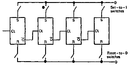 |
Figure 4.13. A pre-settable down-counter.
Each flip-flop can have its Q output set to 0 or 1, so that the down-count
started from this set number |
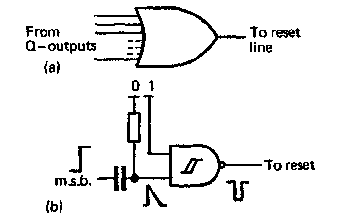 |
Figure 4.14. Ways of detecting the all-0
state: (a) using a multioutput OR gate whose output is 0 only when all inputs
are zero, (b) using a differentiating circuft to detect the positive pulse
at the end of a count |
Down counting is a much more flexible system because the state
which is to be detected is always the same - the all 0s or the change to
all-1s. The number of the count is decided by the binary number which is
set up on the counter before starting. This is, in fact, a primitive type
of programming in which the count is decided by the number loaded
(software) rather than by the connections within the counter
(hardware).
The next step that is possible with a ripple counter is to enable counting
to go in either direction. Since the only difference between the up-counts
and the down-counts is the use of Q for up-counts and Q for down counts,
gates can be connected between counter stages to route the selected output
to the next clock input. Figure 4.15 shows one possible system.
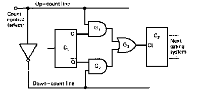 |
Figure 4.15. An up/down counting system,
showing only one pair of flip-flops. The two control lines are driven by
a single input using an inverter to ensure that one line is always the complement
of the other |
Each output of one flip-flop is taken to the input of a two-input
AND gate whose other input is connected to a line.The AND gates which have
inputs from the flip-flop Q terminals are connected to the up line, and the
AND gates which have inputs from the flip-flop Q terminals are connected
to the down line. The AND gate outputs are connected to an OR gate which
in turn drives the clock input of the next flip-flop.
When the up line is set (by a control switch) to logic 1 with the down line
at 0, then a 1 at the Q output produces a 1 at the output of the AND gate
G1 and, in turn, a 1 at the output of its OR gate, G3. In this way clock
pulses are connected from the Q output of C1 to the clock input of C2. If
the up line is switched to logic 0, then the output of the AND gate G1 remains
at 0. With the up line held at logic 0 and the down line at logic 1, a 1
pulse at Q will cause a 1 output from G1 which also will cause a 1
output from the OR gate. In this condition the clock pulses into C2 have
been routed from the Q output of C1, so that the count is downwards.
Because the up and down lines must always be inverse, i.e. can never be allowed
to have the same logic voltage, a single control can be used with an inverter
to ensure the correct line voltages, as shown in Figure 4.15. Using
this scheme, a 1 on the 'select' input will ensure down counting and a 0
on the 'select' input will ensure up counting.
A complete i.c. up/down binary four-stage counter using such a scheme is
the 74191. The up/down input pin is set to logic 0 for the up count and to
logic 1 for a down count. Provision is made for each stage of the counter
to be loaded, using the data inputs, A, B, C, D.
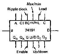 |
A, B,C, D are load inputs, setting or resetting
the flip-flops when the load (L) input is at logic 0
QA,QB,QC,QD are the output
of each F/F |
| Figure 4.16. The 74191
counter which permits presetting of each stage, up or down counting, and
has various outputs which mark the progress of the count |
These are loaded into the flip-flop only when the load pin
is taken to logic 0; the data inputs are ignored at any other time. An additional
control, enable, permits the count to be interrupted. Counting takes
place when the voltage on the enable pin is at 0 and is suspended when the
enable pin voltage is at 1. The use of enable does not reset the counter;
if enable is taken high during a count, the count will continue whenever
the enable input is taken low again.
Two useful outputs from this particular chip are the max/ min and
ripple clock pins. The max/min output is a positive-going pulse longer
than the clock pulse at each change-over of the most significant bit of the
count - the max/min pulses are arranged so that one has a trailing edge
coinciding with the leading edge and the next has its trailing edge coinciding
with the trailing edge of the QD pulse (Figure
4.17).
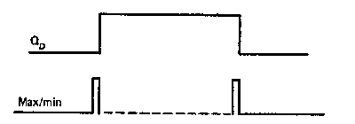 |
Figure 4.17. The max/min output of the
74191 |
This can be used for detecting the end of a count, maximum
or minimum. The ripple clock output is a negative-going pulse at the end
of a count (but of normal clock pulse width) which can be used as a carry
to the next stage of counting.
Synchronous counters
The disadvantages of the ripple counter have been noted earlier,
in particular the problem of the time taken for a pulse to ripple through
all the stages of a counter. An alternative method of counting is the
synchronous counter in which each flip-flop is clocked by the same input
pulse so that all changes occur at the same time. The design of the synchronous
counter with a few stages is fairly straightforward, but the procedure becomes
very difficult when a large number of stages is needed. Fortunately, LSI
synchronous counters are available for the most-needed number counts, and
there are alternative methods available for count numbers which are not decimal,
BCD, nor convenient powers of two.
The principle of the synchronous counter is that at each state of the count
the binary numbers present on the outputs of each flip-flop at each count
number are used to set the J and K inputs of the next flip-flop. The pattern
of connections must be correct if the count is to proceed normally.
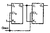
To see how this operates, consider the very simple two-stage counter of
Figure 4.18, and recall the truth table for the J-K flip-flop (Figure
4.7). The state-table alongside the diagram of Figure 4.18 shows
the Q0 and Q1outputs, and also the voltages present
of J1 and K1.
The first clock pulse will have the effect of switching over Cl0,
since J0 and K0 are permanently connected to logic
1.
 |
| Cl |
Q0 |
Q1 |
J1 |
K1 |
| 0 |
0 |
0 |
0 |
0 |
| 1 |
1 |
0 |
1 |
1 |
| 2 |
0 |
1 |
0 |
0 |
| 3 |
1 |
1 |
1 |
1 |
| 4 |
0 |
0 |
0 |
0 |
|
| Figure 4.18. A two-stage
synchronous counter and its state table. The clock pulses are fed to each
flip-flop, and the J K connections determine the action at each clock pulse.
In the state table the values of Q0 and Q1 are those
after the irailing edge of each clock pulse |
Because Q1 (at logic 0) connects to J1
and K1, however, Cl1 will be unaffected by the clock
pulse. Q0 does not switch to logic 1 until the trailing edge of
the clock pulse arrives, by which time J1 and K1 have
'locked-out' - they were at logic 0 at the leading edge of the clock
pulse so that this is the setting which decides the output from
Cl1.
At the next clock pulse, of course, J1 and
K1 are at logic 1, so that the clock input which causes
Q0 to change from 1 to 0 also causes Q1 to change from
0 to 1, giving the binary count 10 (decimal 2). This leaves J1
and K1 set to logic 0, so that the next clock pulse does not affect
Cl1, but changes Cl0 from 0 to 1. The binary count
is now 11, decimal J. With J1 and K1 set to 1 by
Q0, the next clock pulse will switch both flip-flops back to 0
output.
To extend the synchronous counter to more than two stages gating must be
used in addition to the flip-flops. A three-stage counter is shown in Figure
4.19 with an AND gate used to set the Jand K inputs of the third stage.
The effect of this gate is that J2 and K2 are set to
logic 1 only when Q0 and Q1 are both at logic 1.
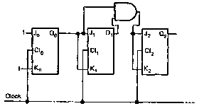 |
Figure 4.19. A three-stage synchronous
counter |
The count therefore proceeds in the way described for the two-stage
counter until Q0 = 1 and Q1 = 1. At this point, the
action of the AND gate holds J2 and K2 at logic 1,
so that the next clock pulse, which sets Q0 and Q1
back to 0, will switch over Q2, giving the count number 100 (decimal
4). The next three pulses have no effect, because the output of the gate
is low, so that Q2 cannot switch over. At decimal 7,Q0
and Q1 are again both at logic 1, so that the eighth pulse once
again switches over C12.
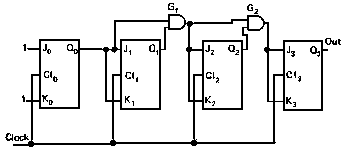 |
Figure 4.20 A four-stage synchronous
counter |
Figure 4.20 shows a four-stage synchronous counter;
the reader 1 is invited to check out the gating to the fourth stage for
himself. Synchronous counters, like ripple counters, can be set to count
in either direction, and a down-count with detection of 0 is, as before,
a simpler method of stopping a count after a definite number. Synchronous
counters can be designed for resetting after a given number and this can
be achieved by gating the J and K inputs only, but the procedure is far from
simple when the counters contain large numbers of stages. The usual design
method is to write the state of each Q output for each count number, then
the J and K numbers for the next state, so that gates can be arranged
to produce the right combination of J and K settings. It's a tedious process,
and the graphical version, called Karnaugh mapping, is only really
helpful when fairly small numbers of stages are being designed, or when codes
other than straight-forward binary are to be used.
Counters seldom have to be constructed from flip-flops, since ready-made
i.c. counters are available. In addition, shift registers (see Chapter 5)
can be used as counters for most counting scales. Nevertheless, constructing
a counter from flip-flops is a useful exercise because the action can be
checked and traced - this is seldom possible when an i.c. is used!
Practical work
Practical work on counters requires a source of clock pulses. A debounced
push-button switch is useful when the action of each clock pulse needs to
be examined; a low frequency oscillator is more useful when higher speed
clocking is needed. One of the most useful practical introductions to counter
techniques is the 7476 dual J-K flip-flop - this i.c. is low-priced, and
easy to use. The pinout diagram is shown in Figure 4.21. For most
low-speed counter applications, the preset and reset pins can be left floating
- if they are connected to common lines care must be taken to ensure that
they can never both be taken low.
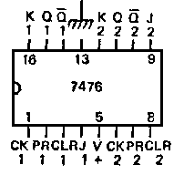 |
CK-clock
PR -preset (set)
CLR - clear (reset)
|
Figure 4.21. Pinout of the 7476 J-K
dual flip flop |
The whole range of counters can be built up using 7476 J-K
flip-flops; if a four-bit synchronous counter is to be investigated, the
74168 is a synchronous up/down counter. The pinout is shown in Figure
4.22.
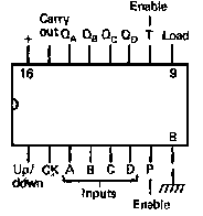 |
Enable inputs P and T must be low for counting
to continue
The trailing edge of the carry out coincides with the leading edge and trailing
edge of Q0
Inputs A,B,C,D allow the counter to be set to any 4-bit number when the load
input is at logic 0 |
Figure 4.22. Pinout of the 74168
counter |
The counting direction is upwards when the up/down pin is at
logic 1, and in the downward direction when low. The enable inputs, labelled
'P' and 'T' form a gate which inhibits counting when both P and T
are high.
|