A shift register is a circuit which uses flip-flops
connected in line so that each bit which is stored at the Q output is shifted
to the next flip-flop in line at each clock pulse. The clock pulses are taken
to all of the flip-flops in the register, so that the action is synchronous.
Any type of flip-flop whose action is suitable (edge-triggered rather than
the latching or 'transparent' type) can be used, and Figure 5.1 shows
typical circuits making use of edge-triggered D-types, clocked R-S types,
and master-slave J-K flip-flops.
To understand the operation of these circuits, recall the truth table for
each flip-flop, together with the 'lockout' action which ensures that a
switchover of the output occurs too late after the leading edge of the clock
pulse to affect the next flip-flop, whatever type of flip-flop from the list
above is used. Imagine that all the circuits of Figure 5.1 have been
reset so that each Q output is set to 0, and that the data input of flip-flop
0 is at logic 1 in each case.
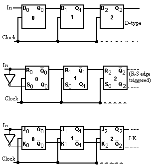 |
| Figure 5.1. Shift-register circuits, using three
different types of flip-flop. Note that it is the Q output of the
R-S flip-flop which drives the next R input |
The D-type flip-flop, with a 1 at its D input, will switch over at the leading
edge of the clock pulse, but the delay will ensure that its Q output does
not affect the input of the next flip-flop and so alter the Q1 output after
the leading edge of the clock pulse. Similarly, the R = 1, S = 0 (because
of the inverter) input of the R-S type ensures that Q0= 0,
Q0 = 1 shortly after the leading edge of the clock pulse,
but with no effect on flip- flop 1. The J-K is similarly affected, with
J0 = 1, K0 = 0 at the time of the first clock pulse,
Q0= 1, and Q1 = 0 at the trailing edge of the clock,
setting up the second J-K flip-flop for the next clock pulse.
Whatever type of flip-flop circuit is used, therefore, the action of the
first clock pulse on the first flip-flop has been to switch the output from
the original setting of logic 0 to logic 1, the voltage of the data input.
At this first clock pulse, each of the other flip-flops in the chain has
had a data input equal to zero from the previous stage (R =1, S= 0 for the
R-S type) so that the first clock pulse leaves each flip-flop except the
first unchanged with zero output. See Figure 5.2.
At the second clock pulse, however, with the data input to the first flip-flop
still at logic 1, the data input to each of the second flip-flops is also
1 (R = 0, S= 1 for the R-S type). At the second clock pulse, therefore, the
output of flip-flop 1 will be unchanged, but the output of flip-flop 2 will
switch over to logic 1. The other flip-flops which follow will be unaffected
because at the leading edge of the clock pulse they have both had zero input.
At the third clock pulse, assuming that the input is still held at logic
1, the third flip-flop of each chain will switch over, leaving the fourth
at logic 0. The fourth flip-flop will, in turn, switch over on the fourth
clock pulse.
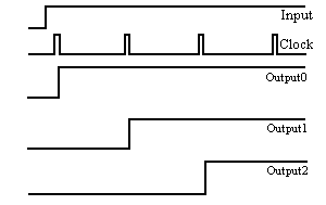 |
| Figure 5.2. The shift action of the register
illustrated |
Shift registers form a very important class of components in all types of
digital circuits. Because the flip-flop output is changed only by a clock
pulse after the input has been changed, the removal of clock pulses, leaving
only the supply voltage present, leaves the output of the flip-flop unchanged
for as long as these conditions are maintained. Each flip-flop can therefore
be made to store a binary digit (or bit) for as long as the power is applied
and the clock pulses are gated out. A set of binary digits can be stored
in a register which has one flip-flop for each digit. We can expect, then,
to find shift registers extensively used wherever there is any reason to
store bits from one operation to another, and several typical register
applications are detailed in this chapter and also in Chapter 7, which deals
with microprocessors.
Before we look at a selection of shift-register circuits, we nee to note
that there are four basic types of register. The type shown in Figure
5.1 is a Serial-In-Serial-Out (SISO) type. The logic voltage at
the input is fed into the shift register at each clock pulse, and can change
in the time between clock pulses. After a number of clock pulses equal to
the number of flip-flops in the register, the same bit is available at the
output. A SISO register used in this way can act as a time delay the bits
at the output are delayed by several clock pulses (equal to the number of
flip-flops) compared to the bits at the input.
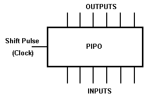 |
Figure 5.3. A PIPO register |
Another basic type of shift register is the Parallel-In-Parallel Out
(PIPO) type (Figure 5.3). In this type, the information (data) bits
are loaded into each flip-flop in parallel, using the set/reset terminals
rather than by clocking. If no clock pulses are applied, of course, the bits
are not shifted, and the readout at the Q terminals is the same as was loaded
in. This use of the register is a convenient method of temporary storage
for a few bits. If clock pulses are applied, then each bit will be shifted
one place at each clock pulse, and the readout will not be identical to the
original data pattern which was loaded in. This leaves the unanswered question
of how the serial input and output are used. One possibility is to connect
the input to logic 0 or logic 1, and to ignore the output. In this form of
operation, the register will fill up with 0s and ls after a complete set
of clock pulses. Another possibility is to rotate, to connect the final output
of the register back to the serial input, so that the register output is
fed back in at each clock pulse, and a complete set of clock pulses leaves
the contents of the register unchanged.
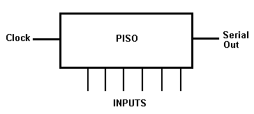 |
Figure 5.4 A PISO register |
The two remaining types of shift register combine serial and parallel methods.
The Parallel-In-Serial-Out (PISO) register (Figure 5.4) uses
the set/reset terminals of a J-K nip-flop to load data bits into each flip-flop
independently and at the same time. The data is then shifted out one bit
at a time when clock pulses are applied. This makes it possible for data
which was present in parallel form (on several lines at the same time) to
be converted to serial form (one bit after another) to be transmitted along
a single line. Conversion to serial form is necessary if the bits are to
be transmitted along telephone lines, recorded on tape, sent to a video monitor
(see Chapter 6) or used to operate a teleprinter.
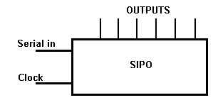 |
Figure 5.5 A SIPO register |
The Serial-In-Parallel-Out (SIPO) register (Figure
5.5) performs the opposite function. In this type data is presented a
bit at a time and is shifted in at each clock pulse. After a complete set
of clock pulses the register is full, and the contents can be read at the
Q terminals or unloaded along a set of parallel lines. In this sense 'unloaded'
means simply that the bits can be used to operate gates or other circuits
- the registers are not changed in any way by this action. Using the SIPO
register, data bits which have been transmitted in sequence from a single
line can be collected to make a 'word' of several bits.
One simple example of the use of a SIPO register is as a counter with decimal
indication, using a l0-stage shift register.
Logic 1 is loaded into the register on the last flip-flop, and logic 0 into
all of the remaining flip-flops. The serial output is then coupled back to
the serial input, as shown in Figure 5.6, and each parallel output
is connected to a display digit (see Chapter 6 for details).
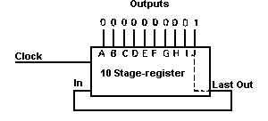 |
Figure 5.6 A decade (decimal) counter using a 10-stage
register - this is an example of a ring counter |
As shown, before a clock pulse arrives the 1 stored in the last flip-flop
illuminates the 0 of the display. The first clock pulse will then shift the
logic 1 into flip-flop A so that the output of F/F A is now logic 1, illuminating
the figure 1. Similarly, the second clock pulse will shift the 1-bit so that
digit 2 is displayed, and so on. A carry to a second stage of counting can
be arranged by connecting the output of the zero counter to the clock input
of another similar register. Since a l0-stage shift register can be made
as a single-chip i.c., this method of decoding a decimal count is simpler
than the binary-to-BCD methods which will be described later, but only if
a suitable display system is available.
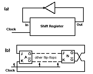 |
Figure 5.7. The Johnson counter (a) is also known
as the 'twisted-ring' counter because of the inversion (b) which can be carried
out by crossing over the Q-J and Q-K connections between the last
flip-flop and the first. When an i.c. shift register is used, this inversion
has to be performed by a separate inverter |
Johnson counters
The Johnson counter is a circuit which uses shift registers to provide
synchronous counting without design complications. High counting speeds are
possible, and the decoding can be comparatively simple, unlike a binary or
BCD counter. The principle of the Johnson counter is to connect a shift register
with the final output connected back to the serial input, but with inversion
(Figure 5.7). Because of the appearance of the
circuit the counter is sometimes referred to as a twisted-ring counter
to distinguish it from the simple ring counter of Figure 5.6.
The simple Johnson counter has a maximum count length of 2n, where n is the
number of flip-flops used in the shift register. This compares with
2n for a binary counter, and n for a simple ring counter.
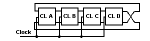
The action of a Johnson counter, as illustrated in Figure 5.8, is
as follows: Imagine that the starting condition is with all the outputs at
zero. The inversion of the final output will therefore place a logic 1 at
the input, so that the first clock pulse loads a 1 into F/F A. At the second
clock pulse the input conditions of F/F A are unchanged and the 1 in F/F
A will be shifted into F/F B. This action continues, loading is into F/F
A each time, until five clock pulses (in this example) result in the register
being filled with 1s. The inversion of the final output now ensures that
a logic 0 is placed at the serial input, so that the next clock pulse will
load a 0 into F/F A and each successive clock pulse will shift the 0 across
and load in another ( until the register is once again filled with 0s.
Figure 5.8 shows the truth table, which also shows the outputs to
be gated in order to detect each stage of the output. Note that each count
number can be detected by a two-input gate.
 |
| Counter pulse number |
QA |
QB |
QC |
QD |
Decoding |
0 |
0 |
0 |
0 |
0 |

 |
1 |
1 |
0 |
0 |
0 |
A |
2 |
1 |
1 |
0 |
0 |
B  |
3 |
1 |
1 |
1 |
0 |
C |
4 |
1 |
1 |
1 |
1 |
A D |
5 |
0 |
1 |
1 |
1 |
B |
6 |
0 |
0 |
1 |
1 |
C |
7 |
0 |
0 |
0 |
1 |
D |
|
Figure 5.8. A four-stage Johnson counter and its truth
table. The decoding column shows what quantities are AND-ed to form the eight
outputs. |
The simple Johnson counter, because the count number is equal to twice the
number of flip-flops used, can be used for even number counts only, since
twice any number is always an even number. To count odd numbers, gate circuits
must be added so that the all-1 state is skipped in each cycle. This can
be done by using the gate to detect the state just before the all-1s state.
For a five-stage register this state is 11110, so a four-input AND gate and
inverter (to invert the 0) are AND-ed to the input. In the example of
nine-counter shown in Figure 5.9 NAND gates are used, so the input
has to be inverted again.
Since the nip-flops of a shift register may go to the logic 1 or to 0 when
power is applied, some method of setting a Johnson counter is needed before
counting can start. If the shift register is of a type which allows each
stage to be cleared (reset), this is a simple solution, particularly if the
reset can be automatically carried out when the power is switched on. Circuits
which do this (based on the use of a monostable) are called initialising
circuits. If this method cannot be used, gating must be arranged so that
the counter will settle into its correct pattern. To ensure that a counter
of more than three stages is self-starting without a clear action, feedback
is needed from more than one stage. For design details, the interested reader
is referred to Texas Instruments' Application Report B102.
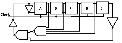 |
Figure 5.9. A five-stage Johnson counter with gating
to detect the State 11110, and so switch a 0 into the input in place of the
1 from stage E which would normally cause the count to go to 11111
|
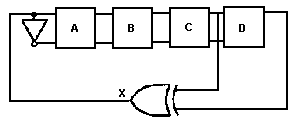 |
Figure 5.10. A maximum length non-binary counter.
The counter flip-flops would normally be part of an integrated shift
regtster |
Other types of synchronous counters using shift registers are possible and
usually easier to design than binary synchronous counters, particularly when
a long count number is needed. The maximum count length which can be obtained
by such methods is only one less than that of a binary counter using the
same number of flip-flops.
The circuit shown in Figure 5.10 uses feedback through an
X-OR gate to the input of the register. The flip-flop
outputs which have to be used to feed the X-OR gate depend on the number
of flip-flops in the register; for three or four stages, only the last two
stages (the most significant bits) need to be used. The circuit for a four-stage
counter is shown in figure 5.10 and the count sequence is shown in
Figure 5.11. Note
that the counting action will stop if the register becomes filled with 0s
at any time, so that a preset (set) input or a gating circuit must be used
to prevent this from happening at switch on.
Count |
A |
B |
C |
D |
X |
1 |
1 |
1 |
1 |
1 |
0 |
2 |
0 |
1 |
1 |
1 |
0 |
3 |
0 |
0 |
1 |
1 |
0 |
4 |
0 |
0 |
0 |
1 |
1 |
5 |
1 |
0 |
0 |
0 |
0 |
6 |
0 |
1 |
0 |
0 |
0 |
7 |
0 |
0 |
1 |
0 |
1 |
8 |
1 |
0 |
0 |
1 |
1 |
9 |
1 |
1 |
0 |
0 |
0 |
10 |
0 |
1 |
1 |
0 |
1 |
11 |
1 |
0 |
1 |
1 |
0 |
12 |
0 |
1 |
0 |
1 |
1 |
13 |
1 |
0 |
1 |
0 |
1 |
14 |
1 |
1 |
0 |
1 |
1 |
15 |
1 |
1 |
1 |
0 |
1 |
Figure 5.11. The count sequence for the circuit of
Figure 5.10
To understand the action, imagine the register filled with 1s. Since the
inputs to the X-OR gate are both ls the output of the gate is 0, and this
0 will be shifted into the first flip-flop of the register. The next counts
have the same action, but at the fourth count the shift action has left only
a single 1 input to the X-OR gate. With this input, the output of the X-OR
gate is also 1, so that a 1 is loaded in at the next count. Meantime, the
inputs to the X-OR gate have gone to 0, so that the next digit loaded in
is 0. This cycle then continues until the first repetition after a count
of decimal 14.
Figure 5.12 shows what stages are needed to feed the X-OR gate for
various numbers of stages of shift registers up to 12. Shorter counts can
be obtained by using additional gating which causes the counter to jump one
or more states. The gating is chosen so that the jump needs only a different
digit loaded into the input. For example, to shorten the count of the circuit
of Figure 5.10 by three places, the count can jump from 1000 to 1100
by loading in an extra 1 - The state 1000 is the only state in which the
outputs of the flip-flops B, C and D are all zero, so that a gate which detects
this state can be OR-ed with the X-OR gate to provide the skip. For longer
counts the gating can sometimes be simplified by using
Boolean algebra
to describe the jump condition.
Number of stages |
Stages fed to X-OR gate |
Count |
|
| 3 |
BC |
7 |
| 4 |
CD |
15 |
| 5 |
CE |
31 |
| 6 |
EF |
63 |
| 7 |
FG |
127 |
| 8 |
DEFH |
255 |
| 9 |
EI |
511 |
| 10 |
GJ |
1023 |
| 11 |
IK |
2047 |
| 12 |
FHL |
4095 |
| Figure 5.12. Connections from the shift
register output, to the X-OR gate for making counters of various lengths
|
Binary, decimal and BCD conversion
Because of its simplicity, binary arithmetic is used extensively in digital
circuits, but displays are generally of decimal numbers (see also Chapter
6). To display decimal numbers some sort of conversion of binary numbers
into BCD is needed. This is not difficulty to carry out, using a shift register,
provided that the rules for converting binary into BCD are known. The rules
are:
-
1) The binary number is shifted, starting with the most
significant bit, into the shift register, whose flip-flops are grouped in
fours.
-
2) Each group of flip-flops in the BCD register represents
a power of 10 in a decimal number, with the binary bits shifted into the
lowest order group first.
-
3) If, before a shift pulse, a group of four flip-flops contains
a number less than five (decimal), shifting takes place normally.
-
4) If the number stored in a group of four flip-flops is
five to nine inclusive, binary three (0011) is added to the stored number
before shifting.
Figure 5.13 shows an example of these rules being applied. The number
to be converted is binary 11010 (decimal 26) and we can imagine the bits
shifted in, most significant bit first, ito a pair of four-bit shift registers
which will eventually contain the BCD numbers. At the first shift, the 1
bit moved into the lower BCD register produces a total of one in this
register, and the second bit shifted in produces a count of three. This does
not require any correction, but the next bit shifted in, a makes the
total 110 (decimal 6) which now requires the correction in the form of adding
011 (decimal 3). This makes he total in the register equal to 1001. The next
shift pulse moves the 1 across to the next BCD register, but with no correction
needed. A 1 is also shifted into the lower register, but again no correction
is needed. The final stage of shifting moves a 0 into each register, and
since this is the last pulse (number of clock pulses equals number of digits
in the number to be converted) no addition is needed to the number in the
lower register even though it has reached 0110 (decimal 6). The figures in
the register are now 0010 0110, the BCD equivalent of 26.
|
|
Shift registers |
Number
|
|
8421 |
8421 |
|
|
|
|
|
11010 |
| First shift |
0 0 0 0 |
0 0 0 1 |
1 0 1 0 |
| Second shift |
0 0 0 0 |
0 0 1 1 |
0 1 0 |
| Third shift |
0 0 0 0 |
0 1 1 0 |
1 0 |
| Add 3 |
0 0 0 0 |
0 0 1 1 |
1 0 |
| Total |
0 0 0 0 |
1 0 0 1 |
1 0 |
| Fourth shift |
0 0 0 1 |
0 0 1 1 |
0 |
| Fifth shift |
0 0 1 0 |
0 1 1 0 |
|
|
| Figure 5.13. Binary-to-BCD conversion,
using the 'add.3' method |
To make these rules operate in the form of hardware, three types of circuit
are needed. One is, as might be expected, a shift register, one is an adder
(the action of an adder is covered in Chapter 7), and the third is a gate
which detects when the content of a group of four BCD digits is five or more.
Figure 5.14 shows the circuit of a four-decade binary-to-BCD converter,
courtesy of Texas Instruments. The shift register is a 74199, which is an
eight-bit PIPO type Pin 23 on this particular circuit is a shift/load input;
a logic 1 level at this pin will cause the i.c. to shift right at each clock
pulse, and with a logic 0 input the register can be parallel-loaded at the
inputs A to H inclusive. For binary-to-BCD conversion pin 23 is maintained
at logic 0.
The binary number is entered at the input of the first 74199, most significant
bit first. This can be done by clocking the digits out of another register,
using a shift direction which allows this most significant bit to be entered
first. At each clock pulse a new bit is entered, and the remaining bits are
shifted (to the right in the diagram of Figure 5.14), but through
the adder, as noted below.
The outputs of each group of four are connected to the 7452 gate i.c.
This contains four AND gates whose inputs (A and B) are connected to an OR
gate which has also an enable input. The inputs from the shift register are
connected so that the output from the 7452 will be 1 for (QA AND
QC) OR (QB AND QC) OR QD equal
to 1. In Boolean algebra, this is QA .QC +
QB .QC + QD. Those are the conditions for
the number stored in the four flip-flops of the shift register to total (decimal)
5 or more, because if QD 1, then decimal 8 is stored, and if
QB and QC are each 1 then the number stored is 6. If
QA and QC are each 1, then the number stored is 5.
For numbers 7 and 9, QC, or QB and QA, will
be l,so that the condition QB and QC equal to 1 is
fulfilled. If 9 is stored (1001) then QD= 1 and QA
= 1 so the output of the gate is also 1.
The effect of a 1 output from the 7452 is applied to the B1 and
B2 inputs of the adder (7483). Now these are the least significant
and next higher bits which wrn be added to the lowest two bits of the number
already stored in the shift register, so that the number 0011 (decimal 3)
is added to the number stored in the register.The action of the shiftiload
pin, remember, has been to allow parallel-loading only; the register does
not shift at each clock pulse. What is happening is that the digits at the
A and B inputs of the adder are added, and the sum presented at the S outputs,
with a carry to the next digit along. Shifting takes place because the sum
of QA and the 7452 gate output is the input to flip-flop B, the
sum of QB and the gate output is the input to flip-flop C, and
so on. When a number of clock pulses equal to the number of bits has been
applied, the registers contain the BCD number which is equivalent to the
binary number.
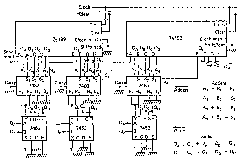 |
| Figure 5.14. Carrying out a binary-to-BCD conversion
using shift registers,adders and gates |
Another method of binary-to-BCD conversion uses an i.c. developed
for the purpose, the 74185. Since this i.c. is a memory rather than a shift
register it wrn not be dealt with in detail here.
Converting from BCD to binary is equally important, because normally a decimal
keyboard will be arranged to give a BCD output of each digit and this output
total must be converted into pure binary form unless circuits for performing
BCD arithmetic are available. As might be expected from the action which
is required to convert binary into BCD, the conversion of BCD into binary
involves shifting and subtraction. The digits of the BCD number are, of course,
grouped into fours and shifted right at each clock pulse. When a logic 1
crosses from one group of four to the next, decimal 3 (0011) has to be
subtracted. This is done by adding the 2's complement form of 3, 1101 in
BCD form, and discarding any carry bit. The steps in a typical conversion
are shown in detail in Figure 5.15. The number to be converted in
this example is 001 0101. Figure 5. 15 shows this written in two groups;
in practice, of course, an eight-bit shift register could hold all of the
digits, but could be used only if it were possible to perform the addition
of 1101 at the appropriate times.
At the first shift, a 1 is moved from the higher digit group to the lower
digit group, and another 1 is moved out of the BCD lower register into the
answer register. In accordance with the rules of conversion, 1101 is now
added to the BCD number in the lower digit group, and the carry is ignored.
Note that nothing is added to the digit which has been shifted into the answer
register because this is no longer a bit of the BCD number.
|
|
BCD
high digit |
BCD
low digit |
Answer register |
|
|
0 0 1 1 |
0 1 0 1 |
|
| 1st shift |
0 0 01 |
1 0 1 0 |
1 |
| - 3 |
|
1 1 0 1 |
1 |
| Ignore Carry |
|
0 1 1 1 |
1 |
| 2nd shift |
0 0 0 0 |
1 0 1 1 |
1 1 |
| - 3 |
|
1 1 0 1 |
1 1 |
| Ignore Carry |
|
1 0 0 0 |
1 1 |
| 3rd shift |
0 0 0 0 |
0 1 0 0 |
0 1 1 |
| 4th shift |
|
0 0 1 0 |
0 0 1 1 |
| 5th shift |
|
0 0 0 1 |
0 0 0 1 1 |
| 6th shift |
|
0 0 0 0 |
1 0 0 0 1 1 |
| 7th shift |
|
0 0 0 0 |
0 1 0 0 0 1 1 |
| 8th shift |
|
0 0 0 0 |
0 0 1 0 0 0 1 1 final result |
|
| Figure 5.15.BCD-to-binary conversion,
using the 'subtract.3' method |
The next clock pulse shifts anothcr 1 into the lower digit register, and
1101 has to be added to this register again,ignoring the carry. All of the
1s have now been shifted out of the higher register, so that all the remaining
steps consist of right-shifts only until all eight pulses have been used.
The final result is 00100011, binary 35.
Figure 5.16 shows a circuit which carries out the conversion for a
four decade comiter. The 74199 is an eight-bit PIPO shift register with
shift/load control as dsecribed earlier.
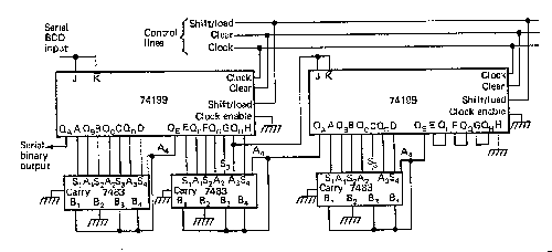 |
| Figure 5.16. Carrying out a BCD-to-binary conversion
using shift registers and adders |
|