| Simple combinational or latching logic circuits operate
immediately on their inputs, involving no time other than the small delay
caused by each gate. A clocked circuit introduces a completely new idea to
logic circuits - the idea that all operations take place during the short
time of a voltage pulse called the clock pulse. The use of a clock pulse
is essential to sequential logic circuits because the clock pulse sets the
time between the steps of a sequence.
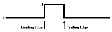 |
Figure 3.1. A typical clock
pulse |
A typical clock pulse is of the form illustrated in Figure 3.1. Between
clock pulses the voltage level is logic 0, and at the leading edge of the
clock pulse the voltage rises abruptly to logic 1. The time needed for this
voltage rise is called the rise time, and will be a time of several nanoseconds.
The voltage remains at logic 1 for a time called the pulse width, and then
returns to logic 0 in a time called the fall time. Circuits which make use
of clock pulses will operate on either the leading edge or the traillng edge
of the clock pulse.
Figure 3.2 is of a clocked R-S latch. The truth table for this circuit
shows the output values before and after the clock pulse. The important
difference between this design and the simple R-S latch is that the output
does not change until the clock pulse arrives, and then the output remains
unchanged (latched) until the next clock pulse arrives, assuming that the
input has not changed in that time.
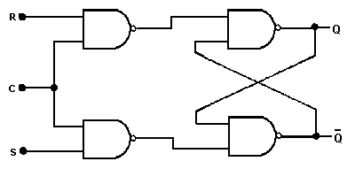
Qn-1 = output before clock pulse
Qn = output after clock pulse |
| A |
B |
Qn-1 |
Qn |
| 1 |
1 |
must not be used |
| 0 |
1 |
X |
0 |
| 0 |
0 |
0 |
0 |
| 1 |
0 |
X |
1 |
| 0 |
0 |
1 |
1 |
|
| Figure 3.1. A clocked
R-S flip-flop. While the clock input is low the inputs to the flip-flop gates
are both high, keeping the outputs in the state to which they were previously
set. Changes at the R and S inputs have no effect until the clock input goes
high. In the truth table, X means 'don't eare' -the input may be either 1
or 0 |
A clocked latch or flip-flop such as this example will act
as a temporary store for a binary digit, and it is particularly useful when
a fast-changing output, such as that of a calculator,has to feed information
to a slow operating device such as a printer. By using the slow device to
generate a clock pulse whenever it is ready for more information, the latch
can be used to hold information until it is needed. In microprocessor circuits
eight-bit latches are very often used for such a purpose.
Clocking is essential for LSI circuits because signals reaching a point in
the circuit may have come through different numbers of gates thereby causing
different delays. By holding back the action until a clock pulse arrives,
and making sure that the time between clock pulses is always more than the
greatest possible delay that a signal can suffer, all the problems caused
by signal delays disappear.
The shape of clock pulses is important. The circuits to which clock pulses
may be applied include high-gain amplifier which are active as amplifiers
only during the time when they are switching over between logic 0 and logic
1. If this time is not very short (around 35 ns) these amplifier circuits
may oscillate during the changeover, thus generating a few clock pulses of
their own. These false pulses can, in turn, be carried around the circuit
causing incorrect operation.
Many clocked circuits specify maximum rise and fall times for the clock pulses,
and correct operation cannot be guaranteed if these times are exceeded. The
time that is specified is that taken for the voltage to rise or fall between
the 10% and 90% levels. For a system using a 5 V signal, for example, the
rise time would be the time taken for the voltage to change from 10% of 5.0V
(=0.5 V) to 90% of 5.0V (= 4.5 V), and the fall time would, of course, be
the time needed for the voltage to fall from 4.5 V to 0.5 V.
Another cause of false pulses is the mechanical switch. When mechanical switches
are used to test gates, as was done in the previous chapter, no problems
arise because the final result is read from the l.e.d.s. When a switch is
used to generate clock pulses, however, or any pulses which are to be counted,
then the problem of contact bounce arises.
The materials of a mechanical switch are springy, so that the controls will
bounce a few times when closed by a mechanical switch thereby causing several
pulses, one at each bounce, and if the switch is used to generate clock pulses
then each bounce pulse will count as a clock pulse.
Wherever a mechanical switch is used, therefore, it must be connected to
a circuit called a debouncing circuit which removes the additional
pulses caused by the bouncing contacts.
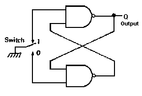 |
| Figure 3.3. Using an R-S flip flop
circuit to 'debounce' a switch. This is called a 'hardware debounce.' In
microprocessor circuits debouncing is carried out by programming a time delay
before the switch value is read - this is a software debounce |
One such circuit, as shown in Figure 3.3, uses a single-pole
two-way switch together with two NAND gates arranged as an R-S latch. The
action is as follows:
With the switch in the 1 position, the R input of the R-S latch is connected
to logic 0, and the S input is at logic 1. This produces a 1 output
at Q. When the switch is changed over, the first part of the action of the
switch causes both R and S contacts to be broken, so that both inputs will
be at logic 1.From the truth table for the R-S latch (Figure 2.17)
this does not affect the output, and there is no effect either if the switch
leaf bounces back against the 1 contact. When the swltch leaf first makes
contact with the 0 connection, the effect is to connect the S input to logic
0. This immediately switches the latch to output 0, because the R input is
at logic 1 If the switch bounces open again, the effect is simply to allow
both Rand S input to rise to logic 1, keeping the output unchanged.
Another type of debouncing circuit is shown in Figure 3.4. This method
makes use of a Schmitt input circuit which can be obtained associated with
NAND gates (7413, 74132) or inverters (7414). A Schmitt circuit has what
is called backlash, that is it will switch in either direction but
not at the same voltages. For example, a Schmitt input may switch over in
the direction at +4.0 V, but will not switch back until + 1.0 V has been
reached. The speed of the switchover is governed entirely by the circuits
inside the device, so that a very fast rise or fall of voltage will be generated
no matter how slowly the input voltage changes.
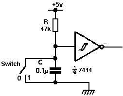 |
| Figure 3.4. Another type of hardware
debounce using a Schmitt trigger gate, one of the six Schmitt inverters in
the 7414 package. The symbol shown lunde the inverter symbol indicates Schmitt
action |
In the circuit of Figure 3.4, the switch is a single
pole on/off type and it is connected to a capacitor and resistor as shown;
With the switch open, the connection of R to +5.0 V ensures that the input
of the inverter or gate is logic 1, so that the output is at logic 0. When
the switch closes, the first touch of the switch contacts discharges C, so
that the input voltage drops to logic 0, making the inverter output switch
over to logic 1. If the switch contacts now bounce open again, the input
of the inverter cannot immediately rise to a voltage which will cause
the output to switch, because of the time needed for capacitor C to change.
The values of R and C are chosen so that the capacitor cannot charge to a
voltage sufficient to change over the inverter in the time of one switch-bounce.
Schmitt-trigger input circuits, which are available both in TTL and in CMOS
types, are extremely useful when clock pulses are obtained from transistor
oscillators or other circuits which do not use digital circuitry. Any shape
of wave, for example, whose amplitude is limited to 5.0 V, will switch a
Schmitt circuit so as to produce clock pulses whose rise and fall times are
suitable for operating other TTL or CMOS circuits. Fast rise times are not
as important for the correct operation of CMOS circuits as they are for TTL
ciruits, but better shaped clock pulses are always an advantage. The inputs
may be rectified a.c., sinewave, or any other waveshape provided that the
amplitude does not exceed the maximum input amplitude permitted for the circuit.
If the signals used to convert to clock pulses are obtained from the same
supply voltage as that used for the digital circuits, no problem of limiting
amplitude will arise. Input signals of various types,however, often come
f'rom quite different types of circuits operating at different voltages,
and are capable of damaging the inputs of digital circuits if applied directly.
These inputs need not necessarily be clock inputs - any input to a digital
circuit will have to be limited so as not to exceed the normal 1 and 0 limits
for the type of circuits that is used.
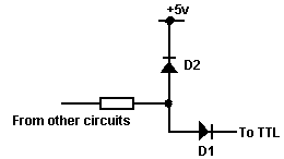 |
| Figure 3.5. An interface circuit
which limits the amplitude of a pulse, obtained from other circuits, to the
5.0 V needed for TTL |
One method of limiting amplitude is shown in Figure
3.5 using diodes. Diode D1 will conduct only when the signal
voltage is above 0.5v,so that the input of the digital circuit is protected
against negative input signals. Diode D2 will conduct if the signal
exceeds 5v,so that the voltage applied to the diode D1 cannot exceed
5.5v. This in turn ensures that the input to the digital circuit cannot exceed
5.0v because of the 0.5 drop across the conducting diode.
Another method uses a transistor as a voltage limiter. With
the collector of the transistor fed from a +5.0 V supply, the voltage at
the collector must swing between +5.0 V (transistor cut-off) and 0.2 V
(transistor fully conducting). A resistor in series with the base input prevents
excessive driving currents, and small capacitance in parallel with this input
resistor prevents the edges of pulses from becoming excessively rounded by
the capacitance between the base and the emitter. The circuit can be used
in two forms: on the n-p-n form a sharp negative leading edge is created;
the p-n-p form creates a sharp positive leading edge.
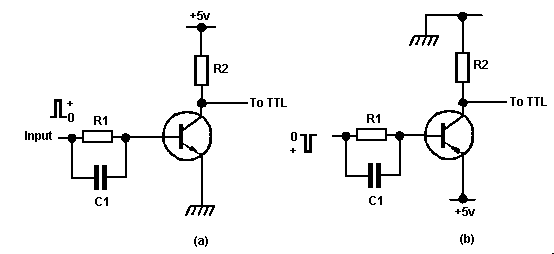 |
Figure 3.6. A transistor interface:
(a) n-p-n, (b) p-n-p |
Generating clock pulses
Clock pulses for circuits which are clocked at high speed usually have to
be generated, unless pulses from other sources (such as the mains supply)
can be used. A clock pulse generator circuit can make use of transistors,
digital or linear i.c.s, provided that the same power supplies can be used
and that the pulse will be of suitable rise and fall time. A linear i.c.
circuit which is very often used along with digital circuits as a source
of clock pulses is the 555 timer. Figure 3.7 shows a 555 times circuit
which generates clock pulses whose frequency can be varied by changing the
setting of VRl. The clock pulses produced by this circuit are sharp enough
to be suitable for CMOS digital circuits, but a TTL buffer circuit is needed
if TTL circuits are to be driven. Using a Schmitt buffer, such as one part
of the Hex Inverter 7414, will ensure that the output pulses have short rise
and fall times and are able to drive 10 input circuits.
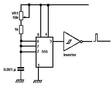 |
Figure 3.7. A clock pulse generator using
the 555 timer. The output from the timer i.c. is inverted so that the short
flyback pulse of the timer is used as a clock pulse-pulse |
An alternative method of obtaining clock pulses is to use a
digital oscillator circuit. Oscillators can be made using NAND or NOR gates,
using circuits such as those shown in Figure 3.8. Note that the TTL
circuits need low resistor values, with 1
kW as the maximum value.
This is because the input to a TTL circuit is to the emitter of a transistor
whose base is connected to +5.0 V. A high resistance at the input will prevent
this emitter from reaching the low logic 0 voltage, so that normal switching
is impossible. The current drawn at logic 0 is 1.6 mA so that the 1 k in
series with a TTL input causes the voltage at the input to rise to + 1.6
V, rather high to be reliably taken as logic 0.
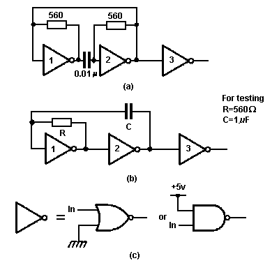 |
Figure 3.8. TTL oscillator circuits.
The i. c.s shown as inverters may also be NOR or NAND gates connected as
indicated. The circuit shown in (b) is much more common |
In the circuit of Figure 3.8(b) the connection of resistor R between
the output and the input of gate 1 creates negative feedback, which reduces
the gain of the gate and causes a wider range of linear operation. Imagine
that the voltage at the input of gate 1 is low. The output of gate 1 will
be high and because gate 2 is also an inverter, its output will be low. Because
of the connections of R, capacitor C will start to charge. One plate is held
at low voltage by the output of gate 2, but the other plate can be charged
by current through R. As the voltage at the input of gate 1 rises, the inverting
action will cause the output voltage of gate 1 to drop, switching gate 2
so that its output is high. The voltage pulse through the capacitor will
cause the input voltage of gate 1 to rise sharply to logic 1, and the capacitor
will now discharge through R because the output of gate 1 is now at logic
0. The times for which the gate voltages are steady are not equal because
when the input of gate 1 is at logic' I the only resistance in circuit is
R. When the input of gate 1 is at logic 0, however, the input resistance
of the gate (which varies from one i.c. to another) is in parallel with R.
The third gate in the circuit sharpens up the rise and fall times of the
wave. Note that when NAND gates are used, unwanted inputs should be connected
to logic 1; when NOR gates are used these other inputs should be connected
to logic 0.
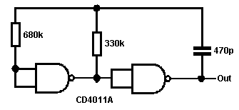 |
Figure 3.9. A typical CMOS oscillator
- NAND gates have been shown, but NOR gates could also be used. The CD4069
hex inverter is also suitable |
The CMOS circuits can use much higher resistance values. TTL
oscillators have a reputation for not always starting when the circuit is
switched on, and oscillators based on the Schmitt trigger digital gates are
preferable, as well as needing fewer sections of an i.c. A typical Schmitt
trigger oscillator is illustrated in Figure 3.10. Imagine that the
input voltage is low. Because the gate is an inverting amplifier the output
will be high,at logic 1. Current flowing through R will charge C, so that
the voltage across C will rise, following the usual capacitor charging curve
with time constant RC. When the input voltage reaches the upper trigger voltage
of the Schmitt circuit, the gate switches over and the output voltage goes
to logic 0.
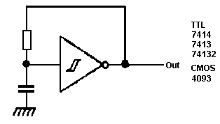 |
Figure 3.10. A Schmitt oscillator circuit.
TTL circuits can use only small resistance values, less than 1k, in this
circuit, but CMOS i.c.s enable much higher resistance values to be used
|
The capacitor now discharges through R but the decrease of voltage
at the input does not affect the output of the gate until the lower trigger
voltage is reached. At this point, the gate switches over again and the action
repeats. The rise and fall times are very short because they are controlled
by the internal circuits of the Schmitt gate, and the clock pulses are of
excellent quality.
The output of the circuit of Figure 3.10 is a square wave with a
mark/space ratio of approximately 1:1 - If very short duration clock pulses
are wanted, a very useful source is a unijunction oscillator. The
circuit is shown in Figure 3.11. The unijunction is a trigger device
which has two connections to a strip of semiconductor, and one to an emitter
junction. When a voltage is placed across the base contacts only a very small
current flows until the voltage of the junction is brought up to a level
which is a constant fraction of the voltage across the base connections.
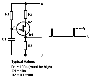 |
Figure 3.11. A unijunction oscillator.
The output is of very short pulses with fast rise and fall times |
When this 'triggering' voltage is reached, the unijunction
conducts freely from emitter to b1 and from b2 to b1 so that large transient
currents can flow. Limiting resistors must be connected to ensure that these
currents are not so large as to damage the unijunction.
In the circuit of Figure 3.11, with the capacitor C1 discharged, the
emitter voltage is low, so the unijunction is not conducting. As Cl charges
through R1, the emitter voltage rises until it reaches the triggering level.
At this voltage, the unjunction becomes a good conductor and Cl discharges
to earth through the emitter-base junction and through R3, with current flowing
through R2 also. The discharge is rapid because of the small value of R3,
and a pulse of short duration is generated. The discharge of the capacitor
also has the effect of switching the unijunction back to its nonconducting
state, so that the process can start again. The pulse from a unijunction
is sharp enough for CMOS use and is usually sufficient for TTL clocking also,
but in order to drive a number of TTL circuits a buffer is desirable, and
a Schmitt inverter such as the 7414 provides both buffering and any sharpening
of the wave-form which may be needed. The pulse frequency is controlled by
the time constant C1xR1.
Keyboard input.
A series of pulses applied to a circuit is a type of input signal called
a serial input. The other type of signal input is the parallel input which
consists of logic signals (either steady voltages or pulses) on a number
of input lines. Parallel inputs are very often used in conjunction with
keyboards, and one simple example of a keyboard action is a decimal keyboard
as might be used in a calculator.
Since digital circuits operate only with binary number inputs, any decimal
figure selected by pressing a key must be converted into a binary number.
The output of a keyboard which carries out this conversion is said to be
BCD (Binary Coded Decimal) because each decimal
figure is separately coded as a binary number.
This is not the same as a binary number which represents the
decimal number. For example, if we are coding the decimal number 35,
pressing the figure 3 key gives binary 0011, then pressing the 5 key gives
0101, so that 35 in BCD is 0011 0101. Each group of four bits represents
one figure of the decimal number. In normal binary coding, 35 is represented
by 100011, a six-bit binary number. For calculating purposes, if we want
to make use of the comparatively simple binary arithmetic, the BCD signals
will have to be converted into binary - this can be done using a converter
i.c. such as the 74184.
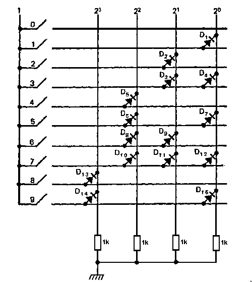 |
Figure 3.12. A diode matrix suitable
for CMOS inputs |
On the keyboard itself, the usual action is for each key to
connect a common line to an output line. The coding to BCD can't be carried
out very simply using a circult called a diode matrix, shown in Figure
3.12. The principle is as follows:
Each binary line is connected through a low value resistor to logic 0, so
that with no input keys depressed all lines are at logic 0. When the key
marked as decimal 1 is depressed, diode Dl is connected between the positive
supply line and the lowest binary line (20). Similarly, depressing
key 2 will connect the positive line to diode D2, making the 21
binary line voltage rise to logic 1. Key 3 connects two diodes D3 and
D4 to both of the binary lines 20 and 21 ,so giving
the correct binary output 0011. Similarly, each key connection raises the
voltages of the appropriate binary lines by conduction through the diodes.
This particular type of diode matrix is simple and uses only fifteen diodes,
but takes rather a lot of current when used with TTL circuits because of
the need to have low resistances in each binary line. CMOS inputs can use
resistors of 100k or more, so that low current operation can be achieved.
The diode matrix of Figure 3.13 is more suitable for use with TTL
circuits. In this type of matrix, which uses 25 diodes, each decimal switch
causes diodes to be connected to logic 0 so that the TTL input current flows
through the diodes. In this type of circuit, however, the output voltage
is 1111 when no switch contacts are made, go the digital circuits must be
capable of identifying this number (decimal 15) as a 'no-input' signal and
gating it out of any counting circuits.
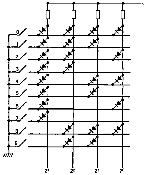 |
Figure 3.13. A diode matrix suitable
for TTL inputs. Several modern keyboards cannot be used this way, and must
be connected to a keyboard encoding i.c. |
Analogue-digital conversion
Imagine a simple thermistor temperature detector (Figure 3.14). The
output of this circuit is a voltage which changes as the temperature changes.
This type of signal can be displayed simply by using a meter, but if we are
to obtain a digital readout we need to convert the varying voltage signal
(which is an analogue signal) into a set of pulses which can be counted (a
digital signal). This requires a circuit called an analogue-to-digital (A-D)
converter, whose input will be the analogue signal, and whose output will
be a series of pulses repeated at intervals.
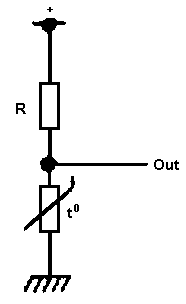 |
Figure 3.14. A simple temperature detector
using a thermistor to give an analogue signal |
The A-D converter needs, in addition to the analogue signal
input, a continuously running clock input which will provide the pulses that
form the output, and a reset signal which starts the conversion all over
again at intervals.
One very common form of A-D converter is known as a ramp type; one
form of this type of converter is shown in block diagram form in Figure
3.15. A start pulse triggers off a sawtooth or ramp signal, and also
sets the R-S flip-flop because of the connection to the S terminal, so that
the Q output of the flip-flop is high. The logic 1 at the Q output of the'
R-S flip-flop is applied to the AND gate, so that clock pulses are fed into
the counter which has been reset to 0 by the start (or command) pulse.
While the level of the ramp voltage is lower than that of the analogue input
voltage, countmg continues, but when the two voltages, ramp and input, are
equal the comparator resets the R-S flip-flop, so that the Q output of the
flip-flop returns to logic 0. This shuts off the AND gate, so stopping the
count. The number that has been counted is now proportional to the analogue
voltage. The next start pulse then resets the counter and starts another
ramp voltage. The start pulses can be derived from the clock pulses or through
a delay circuit operated by the output of the flip-flop.
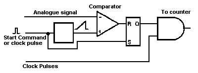 |
Figure 3.15. A block diagram of an A-to-D
converter, using a ramp conversion method. The start, or command, pulse is
at a much lower frequency than the clock pulses, because the ratio of
clock pulse frequency
command pulse frequency is equal to the highest count number that can be
obtained. Note that the R-S flip flop can be used with R=0,S=0 because only
the Q output is used |
The reverse process is also needed. A digital-to-analogue (D-A)
converter will convert a series of pulses into a voltage level, counting
the pulses and using the number of pulses to control the output voltage.
To give one example of the use of such a circuit, a waveform of any shape
can be synthesised by a digital circuit, using the digital output to drive
a D-A converter. The advantage of this type of signal generation as compared
to a conventional analogue type is that any waveform can be generated equally
simply. If the digital circuit contains a microprocessor, for example, the
waveform of the output can be controlled by the instruction program for the
microprocessor, with no alterations needed to the circuit connections.
The principle of most D-A converters is the resistor ladder network,
a typical example of which is shown in Figure 3.16.
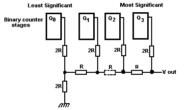 |
Figure 3.16. A D-to-A converter using
a simple ladder network |
Each counter has a resistor connected in its output and taken
to the series chain or ladder, as shown. The resistor values are not particularly
important provided that the ratios are correct, so that the resistors are
labelled in Figure 3.16 as R or 2R -one set of resistors has exactly
twice the resistance value of the other set. These resistance values will
generally be of the order of 1 k, 2 k for TTL circuits, 10 k, 20 k for CMOS.
The least significant bit of the counter is connected to the end of the ladder
network most remote from the output, and the most significant bit of the
counter is connected to the end of the ladder network nearest the output.
With this arrangement, the output voltage will automatically be proportional
to the binary number output by the counter stages.
The reasons for using this network are that only two values of resistance
need to be used, and that the resistance to earth at each point where a counter
is connected is constant when all the counters are at logic 0, equal to 2R.
If, for example, the most significant digit output is 1 and all the others
are 0, the output voltage must be exactly half of the logic 1 voltage, since
the counter feeds through resistance 2R into a load resistance of 2R. When
only the next most significant bit is at 1, the output is then one quarter
of the logic 1 voltage, as can be seen by the arrangement of resistors redrawn
in Figure 3.17. Similarly a 1 at the next digit produces 1/8 of the
logic 1 voltage and so on. Any binary number at the counter outputs will
therefore produce an output voltage in the ladder network proportional to
the number counted.
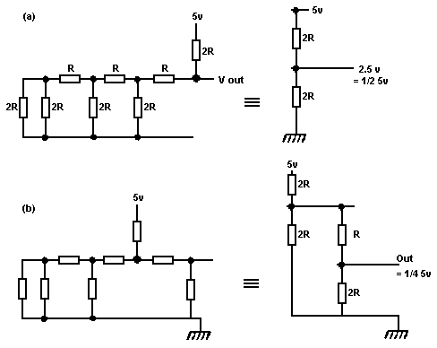 |
Figure 3.17. Examples of the ladder network:
(a) most significant digit 1, others 0 (b) second most significant digit
1, others 0 |
Practical work
The effect of switch bounce is difficult to demonstrate at this stage, but
an R-S debouncing circuit (Figure 3.3) should be made up. This can
be tested by using a crude switch made up from three pieces of wire. The
effect of moving the central wire from one of the end wires to the other,
and then 'bouncing' it, can be noted - if the debouncing circuit is working
correctly then bouncing should have no effect on the output.
Without the use of an oscilloscope the waveforms from digital oscillators
and other clock pulse generators cannot be examined, but the output signals
can be used to drive an amplifier to show that the circuit is oscillating.
The oscillator circuits of Figure 3.8 should be made up, using the
values shown. These values will result in signals which are at audio frequency
so that an audio amplifier/loudspeaker combination will produce a sound when
fed with such signals.
|