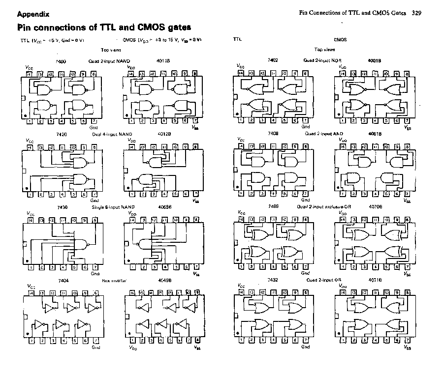
A logic gate is a circuit which uses digital signals
as its inputs and outputs. What makes a circuit a gate is that each output
depends entirely on the signals applied at the inputs. If these input
signals change, then the output signal may also change. Digital circuits
which use logic gates are usually arranged so that a logic 1 appears
at an output only for some definite combination of input signals - for this
reason these circuits are sometimes called combinational logic circuits.
In theory, we could make i.c.s for each and every possible combination of
input signals to produce a 1 output, but this would be wasteful of resources.
In practice, what is done is to make i.c.s which accomplish a few standard
logic operations. From these standard logic i.c.s any combinational logic
circuit can be built up. The microprocessor is an extension of this
idea - a circuit which can perform virtually any logic function.
The action of a standard combinational logic circuit, or of any circuit made
up from these units, can be described in two ways. One way is by the use
of a truth table. A truth table shows what output can be expected
from each possible combination of inputs, so that the action of the circuit
can be readily checked. Another method of describing the action of a circuit
is by Boolean
Algebra. This method is much more concise but less easy for the raw
beginner to interpret, so both methods wrn always be used together in this
book. Boolean algebra, incidentally, was invented long before modern computers.
It is named after George Boole (1815-1864) who devised it as a method
of turning logical statements into algebraic expressions. Little use was
made of this work until Shannon found in 1938 that Boolean algebra could
be usied to analyse relay circuits which carried out the sort of switching
operations we now refer to as 'AND' and 'OR' gates.
AND gate
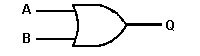
Figure 2.1 shows the symbol, truth table and Boolean expression for
the AND gate, one of the standard logic gates. As the truth table shows,
the output is logic 0 unless both inputs of the two-input gate are
at logic 1. For a three-input AND gate, the output is at logic 1 only when
all three inputs are at logic 1.
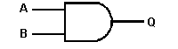
Boolean: A.B= Q Read as A and B gives Q |
| A |
B |
Q |
| 0 |
0 |
0 |
| 0 |
1 |
0 |
| 1 |
0 |
0 |
| 1 |
1 |
1 |
|
| Figure 2.1. A two-input AND gate symbol,
truth-table and Boolean expression. The output is 1 only when both inputs
are at 1 |
As Figure 2.2 shows, the truth table for a gate with
three inputs takes up a lot more space than that for the two-input gate,
and is prohibitively long when four or more inputs are used. The Boolean
expression uses the dot symbol to indicate the AND action so that for a
four-input AND gate the action is A.B.C.D = 1. In words, this means that
the output is 1 only when A AND B AND C AND D inputs are all at 1. Note that
the action of the AND gate can also be illustrated by switches in series,
as shown in Figure 2.3.
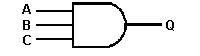
Boolean: A.B.C= Q Read as A and B gives Q |
| A |
B |
C |
Q |
| 0 |
0 |
0 |
0 |
| 0 |
0 |
1 |
0 |
| 0 |
1 |
0 |
0 |
| 0 |
1 |
1 |
0 |
| 1 |
0 |
0 |
0 |
| 1 |
0 |
1 |
0 |
| 1 |
1 |
0 |
0 |
| 1 |
1 |
1 |
1 |
|
| Figure 2.2. A three-input AND gate.
The number of lines of the truth table equals 2n, where n is the
number of gate inputs. The output is 1 only when all the inputs are at 1,
whatever the number of inputs |
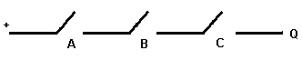 |
Figure 2.3. A switch circuit
which has the same truth table as a three-input AND gate |
For each switch, open = 0, closed 1 |
AND gates are useful for testing for coincidence of binary 1s,
and in circuitry where several factors control an output. For example, a
gas central heating boiler can be switched on (1) when the room thermostat,
the boiler water thermostat, the gas flame detector and the outside temperature
detector are all giving a logic 1 output.
OR gate
The symbol, truth table and Boolean expression for the OR gate are shown
in Figure 2.4. This type of OR gate produces a logic 1 at the output if either
input is at 1 or if both inputs are at 1. For inputs which are all set to
0, the output also is logic 0. As before, the truth table for an OR gate
with more than three inputs is rather bulky, and the action is most easily
summed up by the Boolean expression A + B + C + D+....=1..
Boolean: A + B = Q Read as A or B gives Q |
| A |
B |
Q |
| 0 |
0 |
0 |
| 0 |
1 |
1 |
| 1 |
0 |
1 |
| 1 |
1 |
1 |
|
| Figure 2.4. A two-input OR gate symbol,
truth table and Boolean expression. The output is 1 if any input is at 1
|
The choice of the + sign may look unfortunate at first sight
because it is more natural to associate + with the AND operation, but the
laws of Boolean algebra make the choice of the + sign automatic. The word
'plus' should not be used when reading the expression; for +, read OR at
all tinaes. The Boolean expression A + B + C = 1 is therefore read as A OR
B OR C gives logic 1 at the output. Note that the action of the OR gate can
also be illustrated by switches in parallel, as shown in Figure 2.5. An OR
gate would be used when more than one input may be used to produce an output.
On a central ating system, for example, a logic 1 output may be wanted (to
light the boiler) when the circulating pump starts OR when hot water is
drawn.
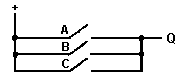 |
Figure 2.5. A switch circuit which
has the same truth table as a three-input OR-gate |
Logic NOT
The NOT gate, inverter, or complementing circuit, illustrated in Figure
2.6, consists simply of an inverting switch whose output is the logic
opposite of the input. In Boolean symbols, the action is represented by drawing
a bar over a letter which represents an input. For example, a signal A passed
into an inverter becomes  ,
meaning that if A were 0, =
1, and for A= l,=0. ,
meaning that if A were 0, =
1, and for A= l,=0.
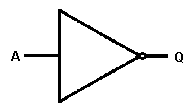
Boolean:
 = Q = Q
Read as inverse (or complement of A is Q, altematively as Q= NOT A |
|
| Figure 2.6. The inverter,
complementer, or NOT gate. This simply inverts the signal at its input. The
small circle at the output indicates inversion - without the circle the symbol
is that of a non-inverting amplifier, or buffer |
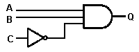
An inverter may be needed in a circuit if previous gates have produced an
output which is of incorrect polarity, or if an input is of incorrect polarity.
For example, if we need an output from a gate when input A = 1 and input
B = 0,then one solution is to use the inverter to convert B = 0 to
 = 1, and then combine
with A in an AND gate (Figure 2.7). = 1, and then combine
with A in an AND gate (Figure 2.7).
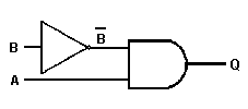
Boolean:
A. = Q = Q |
| A |
B |
Q |
| 0 |
0 |
0 |
| 0 |
1 |
0 |
| 1 |
0 |
1 |
| 1 |
1 |
0 |
|
| Figure 2.7. Using an inverter
to obtain (or implement) a truth table which is not obtained from the AND
or OR gate directly |
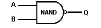
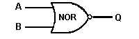
NAND and NOR gates
The combination of the NOT gate with the AND/OR gates produces gate circuits
known as 'NAND' and 'NOR' gates, whose symbols, truth tables and Boolean
expressions are illustrated in Figure 2.8. These gates might seem
of little interest, but they are simpler to construct in integrated form
and have the peculiar advantage that they can be converted more easily into
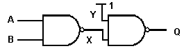
other gates. For example, two NAND gates connected as in Figure 2.9 form
an AND gate; it is not possible to combine two AND gates to form a single
NAND gate. For this reason the NAND/NOR gates are much more common and readily
available than other types. Further examples of the uses of these gate types
in forming other gates are given at the end of this chapter.
 |
Truth Table
| A |
B |
X |
Y |
Q |
| 0 |
0 |
1 |
1 |
0 |
| 0 |
1 |
1 |
1 |
0 |
| 1 |
0 |
1 |
1 |
0 |
| 1 |
1 |
0 |
1 |
1 |
|
| Figure 2.9. Two NAND gates used to
simulate the AND gate. The truth table shows how this happens the second
NAND gate acts as an inverter because one input is held at logic 1 |
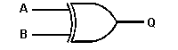
Exclusive-OR
The simple OR gate has a logic 1output for any input or cornbination of inputs
at logic 1- The exclusive-OR (XOR) gate has its output at logic 1 for any
single input at 1 but not for a combination of inputs. The truth table and
symbol are shown in Figure 2.10 along with the Boolean expression
which, in this case, is rather more complex. As it happens, though X-OR gate
i.c.s are obtainable, the Boolean expression contains the clue to a method
of constructing an X-OR gate from other circuits (see later, this chapter).
Discovering gate action
The usefulness of standard gate actions is that any gating logic which may
be needed can be obtained from a suitable combination of these logic circuits.
Designing a logic circuit is not entirely straightforward, but by following
the rules below discovering the action of a circuit is relatively simple:
(1) Label with a letter each separate input for all the gates in the circuit,
and label the output (Q) also.
(2) Draw up a column for each lettered input and final output, setting the
primary inputs (of the first gates in the circuit) apart from the others.
(3)Write rows of logic 0s and 1s for the primary inputs. Each row should
be a binary number, starting with 000------(as many 0s as there are
primary inputs), and increasing by 1 in each row. The total number of rows
should then be 2N, where N is the number of primary inputs. For
example, if N =3 (three primary inputs), 2N = 8,so that the truth
table should have eight rows.
(4) Now write in the output for each primary gate, using the truth tables
for AND, OR, NOT, NAND, NOR, X-OR as required. If these outputs then form
the inputs to other gates, complete the truth tables for these also until
the output column is complete. The result is the complete truth table for
the gating circuit.
 Boolean: Boolean:
 = Q which reduces to
A.B. = Q which reduces to
A.B. = Q, so that the
gating system could be replaced by: = Q, so that the
gating system could be replaced by:
 |
Truth Table
| A |
B |
C |
D |
E |
Q |
| 0 |
0 |
0 |
1 |
0 |
0 |
| 0 |
0 |
1 |
1 |
0 |
0 |
| 0 |
1 |
0 |
1 |
0 |
0 |
| 0 |
1 |
1 |
1 |
1 |
0 |
| 1 |
0 |
0 |
1 |
0 |
0 |
| 1 |
0 |
1 |
1 |
0 |
0 |
| 1 |
1 |
0 |
0 |
0 |
1 |
| 1 |
1 |
1 |
0 |
1 |
0 |
|
| Figure 2.11. Discovering
the truth table for a gate system. The inputs are listed, and the intermediate
signals C and D noted down, knowing the truth tables of the AND and NAND
gates. The final output Q is written down knowing the C and D states and
the truth table for the NOR gate |
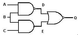
Figure 2.11 shows an example of this technique being
used for a circuit with three primary inputs and one output. When a large
number of primary inputs exist, however, the truth table is very unwieldy,
and a better approach, as usual, is to use Boolean symbols. Each primary
input is labelled A, B,C .... -as before, but the outputs of the primary
gates are then labelled with the Boolean expressions which describe the gate
action. For example, if a NAND gate has inputs A, B, then the output is labelled
 (NOT A-and-B). The
next set of gates is labelled in the same way, using the inputs which have
already been discovered. (NOT A-and-B). The
next set of gates is labelled in the same way, using the inputs which have
already been discovered.
The final expression represents the gate action but may require simplification
to remove terms which are surplus to needs. The laws of Boolean algebra shown
in Table 2.1 can be used to simplify such expressions, and one example
is shown in Figure 2.12. In general, though, these methods are required
only by the professional engineer. The laws are shown only for reference
purposes so that the mathematically inclined reader may make use of them.
The opposite process can usually best be carried out by the use of Boolean
algebra. Once the Boolean expression for the action of a circuit has been
found, the circuit can be sketched out - but finding the Boolean expression
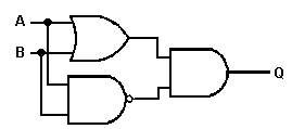
may be a problem. To illustrate how a circuit can be constructed (or implemented)
using the Boolean expression, consider the expression for the X-OR gate of
Figure 2.10:
( ) . (A
+ B) = Q ) . (A
+ B) = Q
(A + B) indicates that an OR gate is needed with A and B as
inputs. () indicates
that a NAND gate is needed, also with A and B as inputs. Finally the outputs
of these gates must be combined in an AND gate, as indicated by the AND dot
between the sets of brackets. The circuit is therefore as indicated in
Figure 2.10(b).
Table 2.1 |
Gate Laws |
AND |
OR |
NOT |
0.0 = 0
0.1 = 0
1.0 = 0
1.1 = 1 |
0+0 = 0
0+1 = 1
1+0 = 1
1+1 = 1 |
_
1=0
_
0=1 |
|
|
| Note: The names shown above are not necessarily those used
by mathematicians |
 |
Boolean: (A.B.C) + A .
(+) =Q
Using De Morgan's theorem becomes:
(A.B. C) + A ( ) = Q ) = Q
Factorising, then:
A. (B.C +) = Q
and since B.C + = 1:
A. 1= Q
so that the circuit could be:
A_______Q
i.e. no gates are needed |
| Figure 2.12. Showing how the use of
Boolean algebra can simplify a logical expression and avoid the use of
unnecessary gates |
This comparatively simple example could also have been drawn
out using only the truth table. The truth table shows that a 1 output must
be obtained when the inputs are OR-ed but not when both inputs are 1. A NAND
gate produces a 0 at the output when both inputs are 1, so that an AND connection
of the NAND gate with an OR gate should give the required expression. Once
a gating arrangement has been designed in this way, it should be checked
by constructing a truth table as shown earlier, unless the number of inputs
is prohibitively large.
A gating system may have to be constructed, however, with only verbal
information. For example, the specification may be: a 1 output is required
when either of inputs A and B is 1, but with inputs C and D 0. No other
combination must give a 1 output. This may be drawn up as a truth table,
but with four inputs 16 rows (24) of inputs will be needed. The
alternative is to construct a Boolean expression directly from the specification.
It is fairly obvious that a 1 at the output for either A or B inputs can
be obtained by using an OR gate, but the output of this gate must produce
a final 1 output only if neither C nor D produces a 1. Now these two inputs
can be fed to a NOR gate, whose output will be 1 only while C and D are both
0. By combining the output of this NOR gate with the output of the OR gate,
using this time an AND gate, the correct function should be obtained. In
Boolean terms the verbal expression would be written:
Q =
(A+B). . .
By De Morgan's Theorem (Table 2.1),
. converts to
( ) so that the expression
becomes ) so that the expression
becomes
Q=(A+B).()
which is the combination of OR and NOR AND-ed as shown above.
One of the fascinations of logic circuit design is that it
cannot entirely be reduced to rules; intuition and experience still
have a part to play. Very often an experienced designer will be able
to avoid difficulties which are not at all obvious to another designer who
is laboriously ploughing through the set procedure.
Race hazards
Logic Systems using signals which change only at widely separated intervals
are seldom troubled by problems arising from the time delay in each gate.
Some logic systems, however, must deal with signals which are at the 1 or
0 levels only for short times of the order of one microsecond or less. Such
high-speed logic presents difficulties arising ftom the time delays in different
circuits which are called race hazards.
Imagine, for example, a NAND gate which generates a negative-going pulse
when its inputs both go to logic 1. The duration of this negative-going
pulse will be the time for which both inputs are positive. Imagine now that
both inputs are pulses
1mS
long. If they coincide exactly then the output pulse will be
1
mS long, but if one input pulse is delayed by 300 ns (1000 ns = 1
mS), then the duration of the output pulse can only be 700 ns. If one
input pulse is delayed by
1mS
or more, then there will be no change in the output at all.
Designing a circuit to eliminate race hazards is not a task for the beginner,
and the main reason for mentioning the problem is to show why logic circuits
which work perfectly at low speeds may fail in curious ways when high pulse
rates are used.
Arithmetic circuits
As the name suggests, arithmetic circuits are intended to carry out the functions
of binary addition, subtraction, multiplication and division. Thanks to the
use of 2's complement arithmetic, subtraction can be carried out by using
a NOT gate and an adding circuit, and the actions of multiplication and division
can also be carried out using only an adder arithmetic circuit combined with
the use of shift registers (Chapter 7).
The addition of two binary numbers on paper is straight-forward, but the
arrangement of logic gates to perform the same action is less simple. The
least-significant bits are easiest to add because there is no carry figure
from an earlier stage.
 |
| A |
B |
S(sum) |
C(carry) |
| 0 |
0 |
0 |
0 |
| 0 |
1 |
1 |
0 |
| 1 |
0 |
1 |
0 |
| 1 |
1 |
0 |
1 |
|
| Figure 2.13. A half-adder
circuit and its truth table |
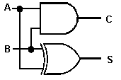
Adding a 1 to a 0 will produce a 1 in the output, but adding will produce
a 0 at the main output and a carry be added to the next pair of bits. The
truth table for this section, called the half-dder, ias therefore as shown
in Figure 2.13. The output in the sum column is the same as would
be expect-ad from an X-OR gate, while the carry out-is the result of an AND
operation on the input parts. A simple half4dder can therefore be constructed
using the gate circuit shown in Figure 2.13. Half-adders can also,
of course, obtained as MSI integrated circuits or as a small part of LSI
circuits.
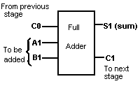
For adding all the pther pairs of bits a more elaborate circuitcalled the
full-adder must be used. The reason is that three inputs are now needed,
two for the bits which are being aded and another one for the carry bit which
has come from previous addition. The truth table is now as shown in
2.14; check this with an addition if there is any uncertainty.
 |
| A1 |
B1 |
C0 |
S1 |
C1 |
| 0 |
0 |
0 |
0 |
0 |
| 0 |
0 |
1 |
1 |
0 |
| 0 |
0 |
0 |
1 |
0 |
| 0 |
1 |
1 |
0 |
1 |
| 1 |
0 |
0 |
1 |
0 |
| 1 |
0 |
1 |
0 |
1 |
| 1 |
1 |
0 |
0 |
1 |
| 1 |
1 |
1 |
1 |
1 |
|
| Figure 2.14. A
full-adder truth table and symbol |
 |
| Figure 2.15. The gating used for
the full-adder |
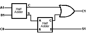
The full-adder is obtainable as a complete MSI i.c., but it
can be constructed from standard gates as shown in Figure 2.15. The
reader should check, using the procedure noted earlier, that this set of
gates will produce the correct truth table.
Negative signs
In discussing arithmetic so far, it has always been assumed that the numbers
are positive. For many digital applications, negative numbers have to be
manipulated, and some way of indicating the sign of such a number is needed.
An obvious method of writing a negative number is to use the 2's complement
of a positive number so that, for example, the number 100101 (decimal 37)
converts to 011011 (decirnal 27). Adding this to a six-bit binary number
produces the same effect as the subtraction of 37; for example, adding to
111001 (decimal 57) gives 010100 (decimal 20) when the seventh bit is discarded
as shown in Figure 2.16.
| 100101 |
Þ |
011011 |
2'scomplement |
| decimal 37 |
|
|
|
|
|
+111001 |
|
|
|
(1)010100
|
|
| Answer: |
010100 |
|
after discarding carry |
Figure 2.16. Two's complement arithmetic |
This is logical enough but the problem is that a digital circuit
cannot distinguish between 011011 meaning decimal 27 and 011011 meaning decimal
-37; and a readout of such binary numbers could not distinguish between the
positive number and the negative one. This is done by using numbers in the
eight-bit byte form, and reserving the most significant bit for indicating
sign. The other seven bits are used for representing number, so that when
this method of writing a signed binary number is used only seven-bit numbers
can be used in one byte. If we want to use larger numbers, we can have each
number represented by a double byte of 16 bits, with the most significant
bit (the 16th) representing the sign. That then leaves 15 bits to represent
numbers, giving a much greater range. Similarly three-byte or four-byte numbers
can be written as signed binary numbers with the most significant bit reserved
for indicating the sign.
The convention as to what value of the most significant bit shall represent
a negative number is easily decided. When, in our earlier example, decimal
37 is written as an eight-bit byte, it becomes 00100101. Converting this
to - 37 by taking the2's complement gives 11011011, so that the most
significant bit is 1, indicating a negative value. The number 01011011 would
be a positive number (decimal +91). A 0 as the most significant bit therefore
indicates a positive number, and a 1 indicates a negative number when this
convention is used.
The advantage of this scheme is that arithmetic can be carried out on these
bytes without any regard to whether the binary numbers represent positive
or negative numbers, and it is only when a final result is obtained that
a 1 in the most significant bit has to be interpreted either as 256 (if only
it e numbers are used) or a negative sign if signed numbers are used.
If signed binary numbers are in use, a 0 as the most significant bit indicates
tbat the following digits represent a positive and the conversion of binary
to decimal is carried out in the usual way. If the most significant bit is
1, however, a negative sign is written, and the following bits are taken
as a 2's complement number. To find the decimal equivalent, therefore, 1
is subtracted from the least significant bit and the number is complemented.
For example, the number 11011011 is read in the following stages:
(a) the MSB indicates a negative sign;
(b) 1011011 has 1 subtracted, giving 1011010;
(c) this is complemented to 0100101;
(d) the decimal equivalent of 0100101 is 37, so that the number represented
by 11011011 is -37
Latching
A combinational logic circuit produces an output which is completely
determined by the inputs, so that a given combination of inputs always produces
the same output. Logic gate circuits can also be combined to produce circuits,
called sequential logic circuits, which behave quite differently.
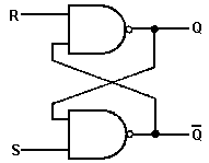
The R=0 S=0 state must be avoided, since
it causes Q = - Q |
A |
B |
Q |
_
Q |
| 0 |
0 |
1* |
1* |
| 0 |
1 |
1 |
0 |
| 1 |
1 |
1 |
0 |
| 1 |
0 |
0 |
1 |
| 1 |
1 |
0 |
1 |
|
| Figure 2.17. The R-S
flip.flop |
The circuit of Figure 2.17 is an example of such a sequential logic
circuit. The circuit uses two NAND gates, cross coupled as shown, with two
inputs and two outputs. At first sight, the truth table seems quite normal,
but repeating some of the inputs demonstrates that the output depends on
the sequence of inputs and not simply on the combination.
For example, with inputs S = 0, R = 1 the output is Q =0, Q= 1 and
changing the inputs to S = 1, R = 1 causes no change. For inputs S = 1, R
= 0 the output is Q = 1,Q = 0, and changing R = 0 to R = 1, so that
S= l,R= 1,again causes no change. For this circuit, therefore, the inputs
S = 1, R = 1can produce either a 1 or a 0 at one output, depending on what
the immediately previous inputs were.
The circuit of Figure 2.17 is called an R-S latch or
flip-flop; the word 'latch' suggests that the output is locked in
place. Latch circuits are used to retain an output for some time even when
the inputs are changing, and such circuits are dealt with more fully in Chapter
4. The simple R-S latch has few applications.
Practical Work
Pracical work on combinational logic circuits can be carried out using the
breadboard along with a few standard i.c.s. In the 74 TTL range, the 7400
quad NAND gate is particularly usweful; its pin diagram is shown in Figure
2.18.
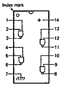 |
| Figure 2.18. The pinout diagram for
the SN7400N quad NAND gate |
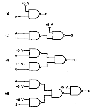 |
| Figure 2.19. A practical exercise
- connecting the gates of a 7400 so as to simutate the actions of other gates
|
Logic circuits can be connected up using switches as inputs,
remembering that an open circuit input on a TTL chip will be at logic 1.
Output states can be detected using l.e.d.s with their series current-imiting
resistors. If the CMOS equivalent (CD4011 A) is used; remember that each
input should have a 1 M resistor permanently connected to earth, and
that the output is best onnected to a transistor/l.e.d. combination as indicated
in figure 1.25.
The circuit arrangements of Figure 2.19 simulate standard gate actions
for which the truth table can be found either practically or by using
the methods of analysis mentioned earlier.
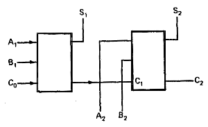
Carry C0 added to A1 added to B1
Þ Sl and carry C1
Carry C1 added to A2 added to B2
Þ
S2 and carry C2 |
| Figure 2.20. The arrangement ofadders
inside the 7482 dual adder |
Figure 2.20 is the internal circuit of the 7482 two-bit full-adder,
with truth table. The carry bit between stages is internally connected and
is not available at the pins.
The Pinout of the i.c. (Figure 2.21) shows what connections have to
be made to switches to give suitable binary inputs,using A1,A2 as one pair
of bits and B1,B2 as the higher order.
Since the circuit of a full adder,a carry into the least significant bits
(C0) can be added and carry out (C2) from the most significant bits can be
detected.
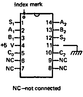
|
| Figure 2.21. Pinout diagram for the
7482 dual adder |
|