An electronic signal consists of a changing
voltage which can be used to represent some non-electronic quantity such
as a sound wave, a picture, a number, a speed etc. The waveshape is
the name given to the appearance of a graph of voltage plotted against time
for such a varying voltage. Some typical wave-shapes are shown in Figure
1.1.
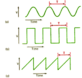 |
| Figure 1.1.
Some typical waveshapes: (a) sinewave, (b) rectangular wave, or square wave
(c) sawtooth. The time period T is measured between two consecutive identical
peaks of the wave |
When a wave contains a repeating patern, as all
the waveforms of Figure 1.1 do, the time for one complete wave is
called the time period (T) and the inverse of this quantity (1/T)
is called the frequency (f).
The amplitude of the wave is its size in volts, and the most useful measurement
is peak-to-peak amplitude, as indicated in Figure 1.2.Measurement
of peak amplitude and r.m.s. amplitude is of little interest in digital
electronics.
Sound waves and televised pictures can be turned
into waveforms in which the shape of the wave is very important, as important
as the frequency or the amplitude. Signals of this ype are called analogue
signals: the word analogue implies that there is a strict correspondence
between the size (amplitude) of for example, the sound wave and the
electrical wave generated from it. Any operation upon an analogue signal
which changes the shape of the waveform is therefore causing distortion,
losing some of the signal information.
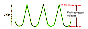 |
| Figure 1.2.
Peak.to-peak amplitude. This is the most useful type of measurement for
digital signals and it is made with an oscilloscope. |
Digital signals convey information using entirely different principles. As
the name suggests, digital signals represent numbers and are a coded way
of carrying information, just as Morse code is a coded method of communicating
words. The waveform of a digital signal is usually that of a steep-sided
pulse (Figure 1.3), but the precise shape is unimportant. The only
important features of a digital waveform are the two levels between which
the voltage changes. These can be called 'high, and 'low', 'on' and 'off',
but are more usually labelled as 1 and 0.
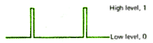 |
| Figure 1.3.
A digital signal, showing voltage levels. |
Since the waveshape of a digital signal is unimportant,
linear amplifiers are not needed for digital signals, and the techniqe of
negative feedback which are so much used for linear amplifiers are
irrelevant. The precise amplitude of signal is also unimportant, provided
that the two voltage levels (0 and 1) are quite different we can arrange
the circuits so that a voltage near to the 0 level will be taken as 0, and
a voltage near the 1 level will be taken as 1.
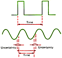 |
| Figure 1.4.
Why fast-rising pulses are used -a time interval can be measured precisely
between sharp pulses, but there is always a considerable uncertainty when
slow-changing waves are used . |
Two portions of the digital signal need to be of
a specified shape however, and these are the leading and trailing edges.
An ideal digital wave would be a rectangular pulse, with the voltage rising
from 0 to 1 instantly and falling from 1 to 0 equally swiftly. In practice,
instantaneous changes are impossible, but rise and fall times measured in
tens of nanoseconds (1 nano second = 10-9, one thousandth of a
millionth of a second) are practical values. These rapid rises and falls
(the rise time is usually more important) are desirable for two reasons,
the first being that digital signals are often used for precise time measurement,
and a rapidly rising voltage is a good starting point; a slowly rising voltage
would introduce considerable uncertainty (Figure 1.4) into a time
reading.
 |
| Figure 1.5.
A slow-changing wave into a digital ie. can cause oscillation during the
output signal . |
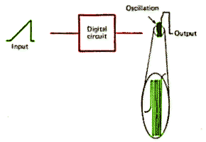
The second reason for using fast rising and falling
pulses is that many digital circuits contain high-gain amplifiers which are
either switched off or fully on, and which can oscillate if they are left
for any significant time biased between the 'off' and 'on' settings, as they
would be in the middle of a slowly changing wave (Figure 1.5). A
significant time as far as starting an oscillation is concerned would be
a microsecond or so.
Logic and counting
Digital circuits are used for many applications, but the types of application
classed as logic or counting are by far the most important. Logic
circuits use the two levels 1 and 0 to mean 'yes' or 'no' respectively as
the answer to a question which can have only two possible answers. Any
process which can be broken down to a series of tests, all of which
have yes/no answers, can be carried out by digital logic. For example, consider
the coin-selecting mechanism of a vending machine. The first test may be
of coin diameter - 'too large or not'? If the answer is 0 for 'not' then
the second test must be 'correct or too small'? By breaking this measurement
down into two go/ no go tests in this way, digital logic can be applied,
and similar tests for weight, metal type, edge milling etc. can be carried
out.
Any logic process can be broken down into a series of simple steps, each
of which will have a 'yes' or 'no' outcome which can be represented by a
1 or 0 output signal. We shall see in the next chapter how such systems can
be designed and analysed.
Even more important than logic circuits is the application of digital methods
of counting. The use of two voltage levels means that only the figures 0
and 1 can be represented, so a counting scale using only these figures must
be used, and the binary scale is one such counting scale.
The binary scale represents numbers, using only the figures 0 and 1, in the
same way as the everyday scale-of-l 0 (denary or decimal scale) uses the
figures 0 to 9. When we write a number such as 684 we interpret it as six
hundreds plus eight tens plus four units, and the separation of the columns
for units, tens and hundreds makes the operations of addition, subtraction,
multiplication and division extremely simple. To be fully persuaded of this,
try adding the Roman numerals CLXII + CCXXIV without converting to
denary scale.
In the denary scale each column represents a power of 10 by which
the figure in the column is multiplied. The power is the number which shows
how many times 10 has to be multiplied by itself to obtain the column value.
For example, when the power of 10 is 2 then the quantity written as
102 is 100, and the column is the hundreds column. Similarly,
the third power of 10 gives l03 or 1000, and by convention we
take 101 = 10 and 100 = 1. We can now number our figure
columns with powers of 10 as in Figure 1.6 using 0 for the units column,
1 for the tens column, 2 for the hundreds column and so on. The figure in
the 100 column (units) is known as the least significant digit; the
one in the highest power column is known as the most significant digit.
The reason for these names is fairly obvious; an error of one or more digits
is much more serious in the highest power column than in the lowest power
column.
| Denary number |
Binary number |
| 103 |
102 |
101 |
100 |
24 |
23 |
22 |
21 |
20 |
| 1000 |
100 |
10 |
units |
16 |
8 |
4 |
2 |
1 |
| 1 |
7 |
4 |
2 |
1 |
0 |
1 |
1 |
0 |
| one thousand |
|
|
|
1 sixteen |
|
|
|
|
| seven hundreds |
|
|
|
0 eight |
|
|
|
|
| four tells |
|
|
|
1 four |
|
|
|
|
| two units |
|
|
|
1 two |
|
|
|
|
|
|
|
|
0 one |
|
|
|
|
Figure 1.6. Denary (scale-of-10) and binary
(scale-of-2) numbers. Each place to the left in a number represents a higher
power of the base number. The base of denary numbers is 10, the base of binary
numbers is 2
A scale of 2 can be drawn up in exactly the same
way using columns representing 20, 21, 22,
23, 24 and so on. The figure placed in each column
must be either a 0 or a 1, since these are the only figures we have. Because
any quantity multiplied by 0 is 0, and any quantity multiplied by 1 is that
quantity unchanged, the conversion of a binary number into denary is simple:
see Figure 1.7 (a).
For example, 101101 has a 1 in each of the columns
20,22,23 and 25 and the value
of 101101 in denary must therefore be 25 + 23
+ 22 + 20. Now, 25 = 32, 23 =
8, 22 = 4, 20. = 1 so that 101101 is equivalent to
32 + 8 + 4 + 1 = 45 in denary. Table 1.1 shows the values of powers
of two up to 223. Converting denary whole numbers to binary is
most easily done using the method shown in Figure 1. 7(b). Figure
1.8 illustrates how the methods shown above may be extended to fractions,
using negative powers to represent quantities such as 0.1 (10-1),
0.01(10-2) and their~binary counterparts 0.5 (2-1),
0.25 (2-2) and so on.
Table 1.1 POWERS OF TWO |
| 20 |
1 |
28 |
256 |
216 |
65 536 |
| 21 |
2 |
29 |
512 |
217 |
131 072 |
| 22 |
4 |
210 |
1024 |
218 |
262 144 |
| 23 |
8 |
211 |
2048 |
219 |
524 288 |
| 24 |
16 |
212 |
4096 |
220 |
1 048 576 |
| 25 |
32 |
213 |
8 192 |
221 |
2 097 152 |
| 26 |
64 |
214 |
16 384 |
222 |
4 194 304 |
| 27 |
128 |
215 |
32768 |
223 |
8 388 608 |
| Note: In computing parlance,
1024 (=210)is known as 1K, as distinct from the usual use of 1k
as 1000 in electronics work. So 8K is 8192 (not 8000), for example. |
When a number is written in the binary scale, each
digit is called a bit (short for binary digit). Groups
of eight such bits are very commonly used in counting, particularly in micro
processors, and are called a byte.
The bit which represents 20 (0 or 1) is called the least significant
bit (LSB), and the bit which represents 27(128) is called the
most significant bit (MSB) of a single byte.
The simple binary code is not the only possible way of using the digits 1
and 0 to represent numbers. The Gray code is used in devices which convert
analogue quantities to digital signals, because it is more error-free. In
a Gray code count, only one digit changes when the count is increased by
1(Table 1.2), but because arithmetic in Gray code is difficult, Gray
code numbers are always converted to binary for processing.
Binary Coded Decimal systems (BCD) use four binary digits to represent
each digit of a decimal number. This can be done by the 8-4-2-1 code, usually
referred to as BCD, in which each decimal digit is converted to its four-bit
binary equivalent, as in Figure 1.9, but another system which is sometimes
used is the Excess-3 code, in which 3 is added to each digit before
converting, as shown in Figure 1.10. The advantage of the Excess-3
code as compared to the 84-2-1 system is that addition and subtraction can
be carried out more easily.
(1) Write down binary number, and note place number
(equal to power of 2) for each 1 in the number. Place numbers start with
0 at the right-hand side:
|
9 |
|
|
6 |
|
|
3 |
2 |
|
0 |
| Example: |
1 |
0 |
0 |
1 |
0 |
0 |
1 |
1 |
0 |
1 |
(2) Now write value of each power of 2 you have
noted, and arrange in a column:
| Example: |
20 |
1 |
|
22 |
4 |
|
23 |
8 |
|
26 |
64 |
|
29 |
512 |
|
|
589 |
(3) . . .and add: Denary equivalent of 1001001101 is 589
Figure 1.7(a). Converting from binary numbers to denary
Number to be converted: 1742
|
Remainders |
| 2)1742 |
|
| 2)871 |
0 |
| 2)435 |
1 |
| 2)217 |
1 |
| 2)108 |
1 |
| 2)54 |
0 |
| 2)27 |
0 |
| 2)13 |
1 |
| 2)6 |
1 |
| 2)3 |
0 |
| 2)1 |
1 |
| 0 |
1 Ü
Read binary number ftom here |
| Binary equivalent of l742 |
1 1 0 1 1 0 0 1 1 1 0 |
Figure 1.7
(b). Converting from denary numbers
to binary. The denary number is divided by 2 and the remainder noted. This
action is repeated until the final division which always leaves a remainder
of 1. The remainders are then read in opposite order, last first, to form
the binary number
| Fractional powers |
| Denary fraction .1111: |
Binary fraction .1011: |
| 10-1 |
10-2 |
10-3 |
10-4 |
.5 |
.25 |
.125 |
.0625 |
| 1 |
1 |
1 |
1 |
2-1 |
2-2 |
2-3 |
2-4 |
| = one tenth |
1 |
0 |
1 |
1 |
| + one hundredth |
= 1 x .5 |
| + one thousandth |
+ 0 x .25 |
| + one ten thousandth |
+ 1 x .125 |
|
|
|
|
+ 1 x .0625 |
|
|
|
|
|
|
|
|
|
|
|
|
0.6875 (in denary) |
Converting denary fractions to binary
Rules: Multiply by 2. Count a 1 on the left-hand side of the decimal point
as a binary 1, count a 0 or 2 as a binary zero. Continue for as long as needed
- many binary fractions never work out finally. Read binary number ftom the
top downwards.
Example
|
0.624 Denary
x2
|
| 1 |
Ü 1.248
.248
x2
|
| 0 |
Ü .496
x2
|
| 0 |
Ü .992
x2
|
| 1 |
Ü 1.984
.984
x2
|
| 1 |
Ü 1.968
.968
x2
|
| 1 |
1.936 |
| Binary fraction is .100111 to six
places (actually equivalent to .596 in denary) |
| Figure 1.8. Fractions - a binary
fraction uses negative powers of 2 after the point, just as a denary fraction
uses negative powers of 10. The conversion of denary fractions into binary
fractions is seldom exact |
Figure 1.8. Fractions - a binary fraction
uses negative powers of 2 after the point, just as a denary fraction uses
negative powers of 10. The conversion of denary fractions into binary fractions
is seldom exact
Table 1.2 GRAY CODE |
Decimal |
Gray code |
| 0 |
0000 |
| 1 |
0001 |
| 2 |
0011 |
| 3 |
0010 |
| 4 |
0110 |
| 5 |
0111 |
| 6 |
0101 |
| 7 |
0100 |
| 8 |
1100 |
| 9 |
1101 |
| 10 |
1111 |
| 11 |
1110 |
| 12 |
1010 |
| 13 |
1011 |
| 14 |
1001 |
|
| Note: The value of the Gray code is
that only one digit changes at each unit of a count. This avoids errors when
some types of analogue.to digital conversions are carried out - for example,
shaft position encoders. The Gray code has to be converted to binary for
arithmetic operations, and i.c.s exist which can carry out the conversion.
|
Denary number: 167
In binary,
| 1 is 0001 |
|
| 6 is 0110 |
using 4 bits for each figure |
| 7 is 0111 |
|
167 is 0001 0110 0111 in BCD Note: In binary. 167
is 10100111
Figure 1.9. The BCD 8-4-2-1 code uses
four bits to represent each figure of a decimal number. This is particularly
suitable for displaying denary numbers (see Chapter 6)
Denary number: 257
Add 3 to each: 5 8 10 Then into 4-bit binary: 0101 1000 1010 Excess-3 number
is 010110001010
Figure 1.10 The Excess.3 code
Simple binary arithmetic
The operations of binary arithmetic can be carried out, on paper, in exactly
the same way as those of denary arithmetic. Addition and subtraction are
illustrated in Figure 1.11, using the carry when a sum exceeds 1 or when
subtracting 1 from 0. Multiplication and division are carried out as shown
in Figure 1.12. These methods are not all particularly easy to apply
to digital circuits. Circuits which perform addition will be dealt with later,
and a simple modification of arithmetic makes subtraction possible without
using a different circuit. The method used is called 2's complement
subtraction and consists of the following process:
(1) The l's complement of the number which is to
be subtracted is formed by exchanging 1s for 0s and 0s for 1s (Figure
1.13).
(2) Another 1 is added to the least significant
bit (LSB).
(3) The 2's complement is now added to the other
number. By using this method, the same circuit which performs addition will
also perform subtraction, provided that the 2's complement of the number
being subtracted can be formed. As we shall see later, forming a 2's complement
is not a difficult circuit task. Multiplication and division are carried
out using shift registers (Chapter 7) in addition to adding circuits.
Addition |
Rules |
111111
Ü carry
1001101
0111011
= 10001000 |
0+0 = 0
1+0 = 1
1+1= 0 carry l
carry l+1+1= l carry l |
Subtraction |
Rules |
110011010
-011010101
=011000101 |
0-0 = 0
1-0 = 0
1-1 =0
0-1 = l carry l
1-1 - carry 1 = 1 carry 1 |
Figure 1.11. Addition and subtraction
in binary numbers
Multiplication |
Rules |
(a) 110011
(b) x 101
110011
000000
110011
= 11111111 |
Write line (a) for each 1 in line
(b), but shifted along the same number of places, then add the lines |
Division |
Rules |
1001
110)110110
110
...
110
110
|
Use exactly the same method as
is used for denary long division 110 110 Figure 1.12. Multiplication and
division in binary numbers |
Figure 1.12. Multiplication in binary
numbers
Number:
l's complement
2's complement
|
10010111
01101000
+ 1
01101001 |
| Subtraction using
2's complement: |
| 1100100 (a) |
Note: |
|
| -0110011(b) |
|
|
| Take 2's complement of (b) |
For |
110001101
- 10111 |
| -1001101 |
rewrite as |
110001101
- 000010111 |
| and add to(a) |
which is |
110001101
+ 111101001 |
1100100
1001101
|
|
(1)101110110 |
| 111101001 |
|
Answer: 101110110 |
and discard the final carry
to get |
|
|
| 0110001 |
|
|
Figure 1.13. Two's complement arithmetic.
The number to be subtracted is 2's complemented and the complement then added
to the other - number. Both numbers must contain the same number of digits
(adding 0s before the first figure of the number if necessary)
 |
| Figure 1.14. Using a
switching circuit to 'sharpen up' a pulse |
Digital switching circuits
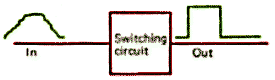
A switching circuit is one whose output voltage shifts rapidly from one extreme
to another when a digital signal is applied to the input. Digital circuits
make use of switching in the way that linear circuits make use of amplification,
with the important difference that the input and output signal amplitudes
of a switching circuit are very often identical. Another important difference
is that the switching circuit will act to 'sharpen up' the leading and trailing
edges of a pulse which has become smoothed out (integrated) in a cable
(Figure 1.14).
A simple voltage switching circuit is shown in Figure 1.15. The transistor
is a bipolar type (in this case, n-p-n), and uses a 330 ohm load resistor
in its collector circuit. The base circuit is unbiased, and connected to
the input through a 4.7
kW resistor
R1 which limits the amount of current that can flow in the base circuit.
A 5.0 V supply line voltage is assumed since this is a standard voltage for
many digital circuits.
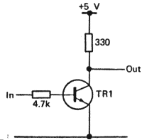 |
Figure 1.15. A simple switching circuit
|
For an input voltage of less than about 0.5 V, the
transistor remains cut-off, so that the collector voltage, which is the output
voltage of the circuit, remains high. Any voltage between 0V and +0.5 V will
therefore count as a 0 input. When the base voltage exceeds +0.5 V, the
transistor will switch on; but the digital signal applied to the input will
not remain at 0.5 V but change abruptly from about 0 V to around +5.0 V.
With +5.0 V at the input, the 4.7
kW input
resistor, along with the base input resistance of the transistor (perhaps
a few hundred ohms) will allow about 1mA to flow into the base (using Ohm's
law and assuming a total of 5.0
kW resistance).
Now the maximum amount of current that can flow in the collector circuit
is limited by the supply voltage and the collector resistor. If we assume
that the collector voltage of the transistor could drop to 0 V, then the
maximum collector current would be 5.0/0.33 = 15.15 mA. To produce this amount
of current in the collector circuit with 1 mA flowing in the base circuit
needs a transistor with a current gain of at least 15, a value which is easily
exceeded. A normal 1 input will therefore ensure that the transistor saturates
- passing as much current as it can in the collector circuit, so that the
collector voltage drops to a very low value, around 0.2 V. The excess current
flowing in the base circuit ensures that the transistor saturates even if
the 1 voltage is less than the 5.0 V we have assumed.
Switching can also be carried out by a MOSFET, as indicated in Figure
1.16. No limiting resistor is needed, because no current flows in the
gate circuit, but a resistor or diode must be connected between gate and
earth to prevent the gate from being affected by 'stray' electrostatic voltages.
Once again, the amount of current which flows in the drain-to-source circuit
is limited by the load resistor, which is usually of several
kW. Once
again, a small change of input voltage causes the output to change between
1 and 0. Ideally, the circuit is arranged so that any voltage below + 1.0
V counts as a 0 and any voltage above 10.5 V (assuming 12.0 V supply) counts
as 1.
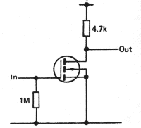 |
Figure 1.16. A simple MOS switching circuit
|
The circuits of Figure 1.15 and 1.16
have, for the sake of simplicity, shown a single stage switching circuit.
Digital circuits generally use switching circuits consisting of several stages,
however, and have rather more power gain than a single stage. The reasons
for using several stages are:
(1) A high gain will ensure that the switchover
is fast.
(2) A high gain will ensure that the switchover is complete for only a small
voltage change at the input.
(3) The output stage of the switching circuit can be arranged so that it
can provide enough signal power to drive several other switching circuits.
Treating these reasons in more detail, Figure
1.17 shows a typical input/output graph for a switching circuit which
uses a 5 V supply. Imagine an input signal which is a voltage rising from
0 V to +5 V in a time of 1
mS, as
indicated. The rise time of this voltage is defined as the time needed for
the voltage to change from 10% to 90% of its final value (5.0 V in this example).
This time, from 0.5 V to 4.5 V, is the time to rise by 4.0 V and is
4/5
mS,
0.8mS.
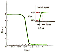 |
Figure 1.17. The output/input graph for
a switching circuit, and how it causes a signal to be sharpened |
Now the input/output graph shows that the output
changes from 4.5 V to 0.5 V for an input change of 0.6 V to 0.7 V. How long
does this take? If the input changes by 5 V in 1
mS, then
it changes by 0.1 V (0.7-0.6 V) in
1.0 x 1.0
5.0mS
which is 0.02
mS. We
would expect that the output change of 4.5 V to 0.5 V would also take this
time, so that the fall time at the output is very much faster than the rise
time at the input.
This, however, is true only if the output of the switching circuit can charge
or discharge the stray capacitances in the circuit at this speed. In addition,
this switching circuit may have to switch on or off several other switching
circuits, each of which will have its own stray capacitance and will also
require some input current. At one time, switching circuits for digital systems
used separately wired transistors, an arrangement called a discrete component
circuit. However, as digital circuits proved their usefulness and demand
grew the number of transistors, and even worse the number of soldered joints,
in a digital circuit became excessive. The use of integrated circuits is
an answer to both of these problems. An integrated circuit (i.c.)
is a complete circuit of transistors and resistors which is constructed on
a tiny chip of silicon, using the same methods as are used to construct
transistors. The first i.c.s contained only a few transistors and resistors,
and are known as SSI (Small Scale Integration) circuits, but as the technology
developed, it soon became possible to construct i.c.s containing the equivalent
of 50 or more transistors. These i.c.s became known as MSI (Medium Scale
Integration) circuits. Later it was discovered that MOSFET circuits could
be fabricated as i.c.s and very large numbers of f.e.t.s could be packed
on one chip. These LSI circuits (Large Scale Integration) can contain
thousands of transistors and resistors arranged into circuits which would
be much too costly and too complex to reproduce using conventional construction
methods.
The availability of i.c.s has led to much greater use of digital circuits
for applications which previously were carried out by either linear circuits
or non-electronic methods. Because the i.c. is made in one sequence of operations
similar to those used for a transistor, it is as easy and cheap to make an
i.c., even an LSI chip, as to make a transistor. The design work on the i.c.
is incomparably more expensive but this can be recovered if enough i.c.s
are made and sold. Reliability is improved because the i.c. can be tested
and its use in place of the separate components it displaces means that fewer
connections have to be made. Most noticeable of all, the size of a circuit
can be greatly reduced, so that it is now possible to design digital equipment
which will fit inside other components. For example, the circuitry needed
to convert a TV receiver into a miniature computer can easily be added and
placed inside the receiver's cabinet. Before LSI, the circuitry for the computer
would have occupied most of the living room. For more details of i.c.s see
the companion Beginner's Guide to Integrated Circuits.
With a few exceptions, i.c.s used for digital circuits are of two types:
TTL and MOS. The TTL types use conventional (bipolar) transistors in integrated
form; the MOS, as the name suggests, use MOSFETs in integrated form, usually
with both p-channel and n-channel types on one chip. Though both 'families'
contain similar circuit functions, the differences between the two types
are important and we shall look at each type in more detail.
TTL digital i.c.s
The name 'TTL' is an acronym for Transistor-Transistor-Logic, a scheme which
has replaced the earlier DTL (Diode-Transistor-Logic) and RTL
(Resistor-Transistor-Logic) circuits. TTL circuits, of which the 74 series
manufactured by Texas Instrumetns is the best-known example, are MSI circuits
which make use of n-p-n transistor structures. The operating voltage is 5.0
V and the design of the circuits is such that this voltage must not be exceeded.
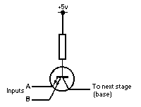 |
Figure 1.18. The input of a typical TTL
circuit is to one emitter of a transistor whose base is returned through
a resistor to the positive supply voltage |
A typical TTL Input stage is shown in Figure
1.18. The input transistor has its base connected to a resistor which
in turn is connected to the +5.0 V supply. The input to the TTL circuit is
to the emitter of this transistor, not to the base, so that this first
stage is a common-base switching circuit. When the input voltage at the emitter
is high, between 4.5 and 5.0 V, the first transistor will not conduct because
the voltage between base and emitter is not high enough. No current will
flow between collector and emitter.
When the voltage at the emitter of the first transistor is low, near 0 volts,
current will flow between the base and the emitter. In the standard series
of TTL circuits, this current is set at 1.6 mA by the value of the resistor
which connects the base to the +5.0 V supply. This current is enough to saturate
the first transistor, meaning that the collector-to-emitter path is low
resistance, as low as can possibly be obtained. Because the emitter of this
transistor is set at 0 V, then, the collector voltage will also be low, no
more than 0.2 V above the emitter voltage.
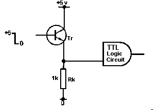 |
Figure 1.19. Driving a TTL circuit from
an emitter-follower - unless Rk is small the TTL circuit will not be switched
off at the input. Values of Rk of 470W
or less are needed |
Because of this construction, examples of which
are illustrated in Chapter 2, the input of any TTL circuit must be driven
from a low impedance source, capable of passing 1.6 mA at a low voltage.
Imagine, for example, a TTL circuit driven from an emitter follower (Figure
1.19). With the emitter fo11ower biased on, the TTL input would be at
logic 1,but switching off the emitter follower would not necessarily turn
off the TTL circuit. The reason is that the resistor Rk might be of too high
a value to let 1.6 mA flow. For example, with Rk =
1kW l,
1.6 mA would cause a drop of 1.6 V, which might not be low enough to let
the TTL circuit switch over. TTL inputs must therefore be driven from circuits
which will allow currents of at least 1.6 mA to flow to earth with a very
small voltage drop. A suitable circuit is, for example, the common emitter
circuit of Figure 1.20.
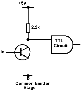 |
Figure 1.20. Driving a TTL circuit from
a common-emitter amplifier - a much more satisfactory way of using a transistor
to drive TTL circuits |
When the base voltage of the transistor is raised
to around 0.6 V, the transistor saturates, so that the resistance between
collector and emitter is very low, and the TTL input is held to about +0.2
V. This is certainly ow enough tp ensure that the TTL input is switched over
to Note, incidentally, that if a TTL input is not connected, it ill 'float'
to a permanent high voltage, logic 1, signal. This hould not, however, be
relied on as a method of keeping an put at logic 1 unless the digital signals
are of low frequency 100 Hz or less). At high frequencies the capacitive
coupling etween one input and others may be enough to cause unwanted input
signals to a disconnected pin, so unused inputs hould be connected through
a 1 kW
resistor to +5 V, or directly connected to earth if a 0 input is needed.
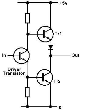 |
Figure 1.21. A typical TTL output circuit.
A few TTL circuits omit Tr1 to form what is called an 'open collector' output
stage (see Chapter 6) |
The type of output stage which is used in TTL circuits
is illustrated in Figure 1.21. Two n-p-n transistors are connected
in series and the output terminal is connected at the point where the emitter
of one transistor joins the collector of the other. To switch this output
to logic 1, transistor Tr has its base voltage taken high, to +5.0V, and
transistor Tr2 simultaneously has its base voltage taken low, to 0 V. The
output terminal now has a low resistance to the +5.0 V supply line, so that
current can pass through a load connected between the output terminal and
earth. In this condition, the output terminal can act as a source of current.
When the circuit switches over, Tr is cut off, with its base voltage low,
and Tr2 is saturated, with its base voltage held at about 0.6 V. In this
state the output terminal is at low voltage logic 0, and current can pass
into the output terminal from a load connected to the +5.0 V line. In this
condition, therefore, the output terminal can act as a sink for current.
In either logic state, a current passing out of or into the output terminal
causes very little change in the voltage at the output terminal. For many
TTL circuits, the maximum current which can pass into or out of the output
terminal is guaranteed as 16 mA. In digital designer's language the output
stage can source or sink a maximum of 16 mA. The importance of this is that
the low impedance and the current handling capacity of this output stage
enables us to use TTL output to drive other circuits. Low current relays,
for example, can be driven directly from a TTL output (subject to the usual
diode protection against the voltage surge occurring when current through
a relay is switched off) and smaller loads such as l.e.d. indicators can
all be driven.
More important, the current sinking ability of an output stage enables one
TTL output to drive up to 10 TTL inputs, each of which needs 1.6 mA to keep
the voltage down to logic 0. In digital designer's language the TTL output
stage has a 'fanout' of 10.
TTL circuits are used in
mainframe (large)
computers because of one considerable advantage - very fast operating
fipeeds. The time needed for a TTL circuit to switch from 0 to 1 or 1 to
0 is about 10 ns, depending on the type of circuit, and even faster speeds
can be obtained using the 74H series of TTL circuits. The price which has
to be paid for high-speed operation is considerable power dissipation, so
that TTL circuits need large current 5.0 V power supplies. The use of a modified
design (Schottky) of TTL, however, enables lower operating currents to be
used, and the 74LS series of TTL circuits (the LS signifying low power Schottky)
can also achieve high operating speeds because the transistors are not allowed
to saturate. The principle which permits this is the construction in integrated
form of a Schottky barrier diode between the base and the collector of each
transistor. A Schottky diode uses an alumlnium-silicon junction and has a
very low forward voltage when conducting, of the order of 0.3 V, so that
such a diode connected between the base and the collector (Figure 1.22)
of a transistor prevents the collector voltage from falling to less than
0.3 V below the base voltage. In this way; when a transistor is switched
on, excessive current flows through the Schottky diode from base to collector
(and so the earth) instead of causing saturation.
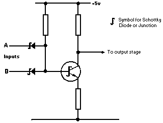 |
| Figure 1.22 A typical Schottky low-power
input stage. The logic switching is done by the diodes, and the transistor,
which also uses Schottky junctions, performspower amplification. Switching
speed can be very high, with much lower currents flowing |
Low power Schottky TTL i.c.s typically dissipate
only one fifth of the power required by the standard TTL circuits; alternatively,
the use of Schottky circuits operating at higher power levels permits switching
times of around 3 ns.
CMOS circuits
Large scale integration requires circuits which dissipate very small amounts
of power, since thousands of transistors have to be accommodated on one chip.
The use of MOS construction enables switching circuits with very low p- and
n-channel MOSFETs, known as Complementary MOS (CMOS) and pioneered
by RCA, has resulted in a complete family of logic circuits.
A typical circuit of a MOS digital i.c. is shown in Figure 1.23. At
the input two f.e.t.s are connected in series, one p-channel and the other
n-channel. The gates are connected together, so that the same signal is applied
to each, and a network of diodes and resistors is arranged to protect the
thin gate insulation from excessive voltage at the input. The action of the
circuit is that a positive voltage at the input will allow current to flow
in the n-channel f.e.t., so making a low resistance connection between
the output terminal and earth. Conversely, a 0 voltage at the input will
allow current to flow in the p-channel f.e.t., so making a low resistance
connection between the output terminal and the positive supply line.
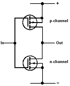 |
| Figure 1.23. A typical CMOS inverter
circuit, omitting the gate protection diodes |
The output terminal is connected to both drains
of the f.e.t.s, so that the f.e.t.s act as voltage amplifiers in each direction.
Several circuits use only one set off f.e.t.s with no separation of input
and output stages, so that the internal circuitry is simpler than that of
TTL circuits. The operating time is longer than TTL, typically 35-100 ns,
but the power dissipation is negligible. In addition, the gate input takes
no measurable current either at the logic 1 or logic 0 voltages, so that
the fanout which can be achieved is limited only by the stray capacitance
of the number of stages which are connected. A fanout of 50 is typical
for many CMOS circuits. On the other hand, the current sinking or sourcing
ability of the output stage is limited to about 0.5 mA, so that interface
circuits are needed if any apart from other CMOS circuits are to be driven.
Even l.e.d. indicator, for example, may have to be driven by an emitter follower
whose base is driven from the CMOS circuit.
CMOS digital circuits can be operated from power supplies ranging from +3.0V
to +12.0V, so that the 5.0Vof theTTL circuits is compatible. In addition,
the low consumption of CMOS circuits permits battery operation, so enabling
the popular 6.0 V or 9.0 V transistor radio batteries to be used. For most
purposes, excluding mainframe computers, CMOS circuits are fast enough and
their tolerance of different supply voltages makes them useful for a variety
of circuits. For experimental use, however, CMOS circuits suffer from the
disadvantage of being readily damaged by stray voltages because of the high
resistance of the gate terminals. The electrostatic voltage on insulators
(including printed circuit boards) or on human hands can be enough to damage
CMOS gates, and the protection circuits are not effective until the i.c.
has been connected into circuit. The most important precautions are:
(1) To connect the i.c.s into circuit only when all components have been
connected. All of the pins must be connected into the circuit.
(2) To use i.c. holders wherever possible.
(3) To use soldering irons which have earthed metal work, and to solder the
earth and supply pins first when connecting the i.c.
(4) To keep the i.c. in its protective plastic foam until it is inserted.
(5) To avoid touching the pins of the i.c.
(6) To treat a complete p.c.b. as carefully as the i.c. itself until the
earth line is permanently connected.
Once connected, a CMOS i.c. is as electrically robust
as any other i.c; the only vulnerable period is that between removing the
i.c. from its protective plastic foam (a conducting material) and connecting
it into its circuit. For this reason, though, TTL i.c.s are preferable for
breadboarding or patchboard work when pins may be open-circuited during changes
of wiring.
Practical work
Like other branches of electronics, digital electronics requires some practical
work for complete understanding. The digital circuits illustrated in this
book can be tested in practice using either TTL or CMOS l.c.s, but the use
of TTL will be more convenient in most cases provided that a stabilised 5.0
V supply available. If only 9.0 V battery power can be obtained, CMOS i.c.s
can be used, but subject to the handling precautions mentioned earlier.
One considerable practical advantage of working with digital ircuits is that
very low-speed operation is possible, so that signal levels can be studied
without the need for an oscilloscope. Since the signal levels are either
1 or 0, the main diagnostic instrument is simply an l.e.d. which glows when
connected to and not when connected to 0. To avoid excessive current, a resistor
must be connected in series when the l.e.d. is used with TTL circuits
(Figure 1.24) and a combination of transistor and resistor used for
CMOS (Figure 1.25).
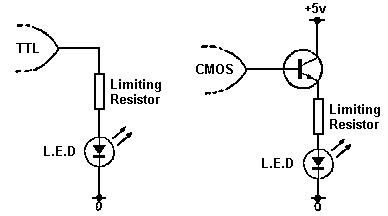 |
| Figure 1.24. An l.e.d. indicator used
with TTL circuits |
Figure 1.23. An l.e.d. indicator used
with a CMOS circuit |
To avoid continual soldering and desoldering, a
solderless breadboard form of construction is recommended. Several types
are available, but the least expensive and the most convenient to use is
the Eurobreadboard (Figure 1.26). This has four columns of contacts,
each column consisting of 25 rows of five contacts each. All the contacts
in a row are connected, and the columns are so arranged that any digital
i.c. package can be placed on the board. The compact shape of the board ensures
that long wire leads are not needed when connections are made from one i.c.
to another. For ease of construction the rows and columns are numbered and
lettered respectively, so that all connections can be made by reference to
this indexing system before the i.c.s are inserted. This enables CMOS i.c.s
to be used.
Figure 1.26. The Eurobreadboard. This is an ideal way of trying
out digital circuits since construction on it is very rapid and all the
components are easily replaceable and re-usable
 |
| Figure 1.27. A typical circuit using
the number/ letter index system of the Eurobreadboard for easy construction.
The number/letter references show where i.c. pins or component leadout wires
plug into. Any of the five plug-in points along one line of the numbered
contact can be used |
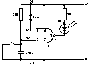
The best technique is to write the index numbers
and letters to the circuit diagram (as shown in Figure 1.27), so that
the circuit can then be constructed with reference to these indexes. If i.c.s
are always placed in the same way, for example a single 16-pin i.c. with
pin 1 on row Al, then construction can be very rapid and circuit changes
can be made rapidly. A useful hint, incidentally, is to connect 1
MW resistors
between all CMOS inputs and earth. If these resistors are left undisturbed,
then rearrangements of the circuit can be made without risk to the CMOS i.c.
and without having to remove the i.c. When TTL i.c.s are used, inputs which
are to be kept at logic 1 can be left floating (unconnected) providing that
the i.c.s are operated with low frequency signals.
|